What Developers Need to Know About FPGA-Based Designs
August 12, 2025
Blog

Specialized semiconductors—particularly flexible and high-efficiency options like Field Programmable Gate Arrays (FPGAs)—have incredible potential to support new developments in computing.
FPGAs make possible the low-latency, low-power, and high-performance capacity devices needed to bring solutions like artificial intelligence (AI) and machine learning (ML) applications, fully optimized data centers, and next-generation networking infrastructure to life.
Given their varied capabilities, FPGAs have opened up a world of new possibilities for engineers and developers. Even so, they are not necessarily a “magic fix” for every development challenge. To use FPGAs to their fullest potential, developers must understand their unique strengths and how to leverage them to balance an array of competing factors throughout the design and build process.

Key Design and Development Considerations
FPGAs are not “plug-and-play” solutions, and capturing their full value depends on having an understanding not just of their potential but also of the variables that determine overall performance:
![]()
- Space and power
From smartphones to in-vehicle Edge sensors, today’s devices—and the resources available to power them—are getting much more compact. This makes implementing chips increasingly difficult, as developers need to account for power and space constraints from day one to ensure they are making the most of what is available. This requires an early understanding of their design limitations and continuous monitoring of how each change or addition affects the system as a whole. Failing to do so can result in routing congestion, energy waste, and the need for unexpected, timely, and costly redesigns.
By paying close attention to limitations from the start and monitoring allocation along the way, developers can proactively ensure that each design decision aligns with the intended outcome of their process. With this approach, the final product will be more likely to meet the desired specifications at both the system and IP levels.
- Thermal limits and waste
Whether a circuit can operate isn’t just a matter of providing enough power; developers also need to account for losses along the way to ensure reliability, longevity, and user safety. With every element added and connection made, leakage currents and static power rise, as does the heat generated within the build.
Mitigating and managing this heat waste must be a top priority, as poor management can result in component failure, performance and efficiency loss, and even potential combustion. As such, understanding and operating within safe thermal limits must be a priority from start to finish.
- Operating speed
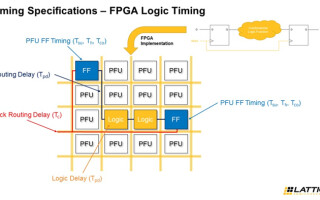
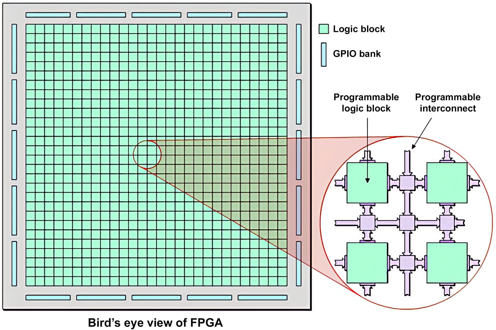
Timing constraints (or “timelinks”) have direct impacts on the placement and routing of a system’s physical design, as trace distance correlates to resistance, energy waste, and other factors. In the long term, the careful consideration of timing constraints helps developers avoid setup and hold time violations and ensure longevity and reliability.
![]()
Similarly, clock domain management and synchronization are key to perfecting an FPGA-based build. Failure to properly manage clock domains alongside traditional time constraints can lead to malfunctions, metastability, and data corruption, as well as impact the efficiency of the build and the circuit's power needs. Adding these functions later on in the process is often more challenging, as clock domain management has a direct impact on resource allocation and overall build requirements. What's more, bugs in this area can be difficult to address and significantly delay development time.
Ultimately, each of these factors impacts the others in some form or another. Higher power needs may increase the potential for heat waste, timing management influences system size and space constraints, and thermal limits restrict computing capacity. This network of interconnected factors means that the system's needs will change with every new design and development decision. This underscores just how crucial identifying and proactively avoiding design challenges is when using semiconductors.
The Importance of Checking Your Work
Before pushing a newly designed system or device into production, developers need to check that these chip-based designs operate as intended. This testing helps reveal any issues that may have been missed in development, enabling proactive remediation and helping avoid timely and expensive post-launch repairs or replacements. But there are also ways to model, test, and improve upon builds along the way.
By assessing system feasibility early and often, developers can ship their finished designs with more confidence and assurance that they’ll get the job done. Advanced simulation software now allows designers to evaluate the feasibility of designs—and assess the impact of changes—before they’re too far along in the process, saving the time and money associated with redesigns and faulty prototypes.
These tools help developers bring their ideas to life even more quickly and enable more innovative and exploratory design processes. They allow engineers to test theories without worrying about waste, as well as template designs for future iterations of chip-based builds.
Leveraging Semiconductors with Confidence
High-performance semiconductor options—like FPGAs—have transformed the way that we build and interact with computing systems. They offer developers the flexibility, power, and processing capacity necessary to create innovative solutions across various industries.
These benefits are only accessible, though, when semiconductors are incorporated into designs in a thoughtful and balanced manner. As technological solutions become more complex and capable, mastering the art of balanced FPGA-based design is the key to unlocking—and sustaining—the next generation of computing.
Chris Sousa is a Regional Sales Manager at Lattice Semiconductor and is based in Raleigh, NC. Chris is responsible for sales and technical solutioning for strategic and channel customers in the Southeast. He was formerly a Field Applications Engineer for two years at Lattice and prior to that, an FAE at Future Electronics. Before becoming an applications engineer, Chris spent 9 years as an FPGA and ASIC engineer in various roles at Actalent Services, Sentec UK, Xylem, and Palo Alto Networks.


