Just do each truth table for every gate. If you know the input, and know how a certain gate operates (NAND in this case) one can always compute the output. Repeat for each stage.
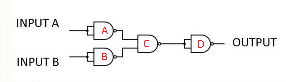
Starting with what I've labeled "Gate A" what if the input is 0, than both inputs to the NAND are 0, which means its output is 1. I've marked it in the chart. Repeat for an input of both 1's and repeat for gate B.
Now you have both inputs to gate C. Since you know the inputs to gate C you can write in the outputs of gate C for all states (Column C).

Filling in the question marks should be pretty simple for column D. Know your inputs and logic; find your outputs. Draw a truth table.
Eventually you will start to use shortcuts such as the aforementioned Demorgan's theorem and things like recognizing if a NAND gate only has one input it simplifies to an inverter gate.