This is not a direct answer to your question, but I think it's quite relevant.
A few years ago, we did the same thing. We made little daughter boards that used edge castellations to solder it onto the mother board.
The difficulty was that we had components on the bottom side of the PCB. These were the vital decoupling capacitors needed by the chip.
So the motherboard had very large vias to accommodate these components.
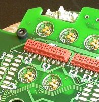
You can see several large round holes in the PCB. Through the holes you can see the capacitors on the flip side of the daughter boards. Since the holes are just large vias, they end up through-plated (our supplier doesn't offer unplated holes), so you have to be careful that the plating doesn't short any pads on the daughter board.
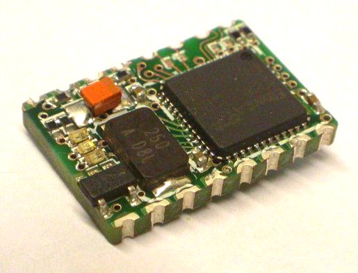
A few thoughts about using pads under the PCB. I assume you mean something like this Telit HE910 module:
Which reflow solders directly onto a PCB. Notice that in the picture the gap between the module and main PCB is not zero, but certainly less than 1mm. Clearly this technique works. Whatever components are inside the module don't mind undergoing an extra reflow process. This is because components can usually survive at least two reflows (once for each side of the board). Since those modules only have components on one side of the PCB, they have almost certainly experienced only one reflow.
Instead of reflow, you might be tempted to use a hot plate to solder a module like this. This would enable you to solder the module down without getting the components inside the module too hot. However, I would advise against this method. At the moment the solder solidifies, the mother PCB will be much hotter than the daughter PCB. As the mother cools and shrinks, it will generate shear forces in the solder joints, and may warp.