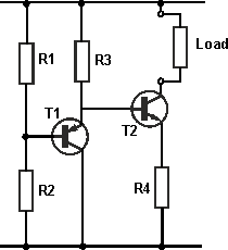
I am working with analysis of BJT current source. I didn't get the explanation of temperature compensation in NPN transistor with PNP and pull up resistor. How does it work actually?
2 Answers
Start with a static analysis.
The voltage at the emitter of T2 is the same (assuming matched Vbe) as that at the base of T1. (The base of T2 is one Vbe above the base of T1, and the emitter of T2 is one Vbe below the voltage at its base).
So I(load) is V(junction R1, R2) / R4 ignoring the base current error term.
Now let us increase the temperature by (for example 10C). Vbe for T1 will reduce by approximately 21mV, therefore pulling the emitter down by this amount.
This will in turn, reduce the base voltage of T2 by the same amount, reducing the forward bias by this same 21mV. T2s Vbe will also have reduced by 21mV, and therefore the voltage at the emitter of T2 remains constant, and there will be no change in the ratio of V / R4, yielding a current that is constant across temperature.
This assumes perfect matching (which you will not get with discrete parts). Even so, the temperature coefficient of the overall circuit will be significantly better than without the compensation.
Update: Added current flow
At some steady state point, the current in R2 is given by (V/(R1+R2)) + Ib(T1). Assuming the base current in T1 is very low compared to the current in R2 due to the divider, we can approximate this as The above without the base current term.
V(R2) is therefore I(R2) x R2.
The current in R3 is ((V+ - V(R2) - 0.6V) / R3) + Ib (T2). Once more, assuming that the base current in T2 is very much less than I(load), we can ignore the base current term. The 0.6V term is because the emitter of T1 is one diode drop above the voltage at the base therefore reducing the voltage across R3 by this amount.
The current in the load is V= V(R2) - 0.6V + 0.6V)/ R4. The two 0.6V terms are due to the fact that two Vbe terms are involved and the emitter of T2 is one diode drop below its base.
Now raise the temperature by 10C. In a transistor, the base emitter voltage will reduce by 2.1mV per degree for some given current, I, so the voltage across each base emitter junction will reduce by 21mV. Now lets drop that in to the currents at each node:
Providing the current in R2 is very much larger than the base current of T1, then the base voltage of T1 will not change, and therefore the emitter voltage will drop by 21mV.
As the emitter voltage of T1 has reduced by 21mV, the base voltage of T2 will also drop by 21mV.
So we have:
The current in R3 is ((V+ - V(R2) - 0.58V) / R3)
The current in the load is V= - V(R2) - 0.58V + 0.58)/ R4.
Note that both base emitter voltages have dropped by equal amounts, effectively cancelling out the error term due to variation of temperature.
- \$\begingroup\$ thanks man!!.It will be more intuitive for me if you explain it through current variations in the circuit, considering cause and its effect. \$\endgroup\$vaibhav– vaibhav2015-11-06 16:15:46 +00:00Commented Nov 6, 2015 at 16:15
Your circuit works best on a fixed supply voltage.In fact current out is almost proportional to supply volts.If T1,R1,R2 were not there and there was just a single resistor instead you would still have a current source but changes in Vbe of T1 would change the current .I have seen this circuit used .Remember that Vbe is temperature dependant.The erbers moll equation derived from semiconductor physics and well documented elsewhere describes this temp variation with reasonable accuracy .The current would rise with temp with the circuit that doesnt have T1. This could be very undesirable in some applications .The role of T1 is to cancel the effects of T2.If T1 and T2 are similiar transistors and thier power disipation is similiar then you can expect reasonable temp stability.
- \$\begingroup\$ thanks . How about current variations during the process? \$\endgroup\$vaibhav– vaibhav2015-11-06 18:09:59 +00:00Commented Nov 6, 2015 at 18:09

