Downloaded 65 times
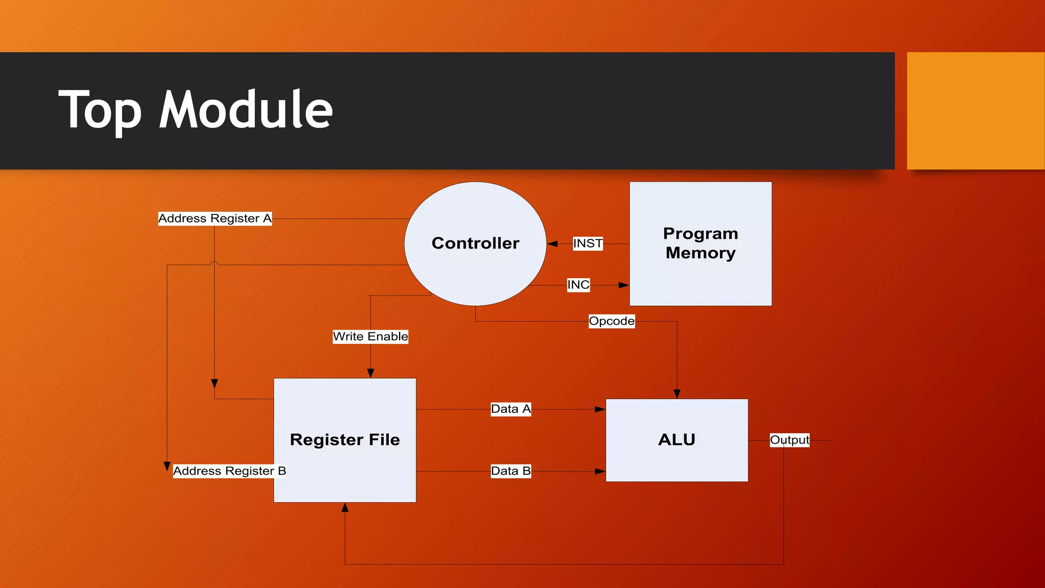
![Top Module module Top_Module(Clk,Reset,PRO_COUNT,INSTRUCTION, AD_A, AD_B, AD_D, A_Out , B_Out,ALU_Out,W_E,OP_CODE); • input Clk , Reset ; • output [15:0] INSTRUCTION; • output [3:0] PRO_COUNT; • output [15:0] A_Out , B_Out ; • output [2:0] AD_A, AD_B, AD_D; • output [15:0] ALU_Out; • output [3:0] OP_CODE; • output W_E ;](https://image.slidesharecdn.com/projectpresentation-150201054124-conversion-gate02/75/Controller-Implementation-in-Verilog-4-2048.jpg)
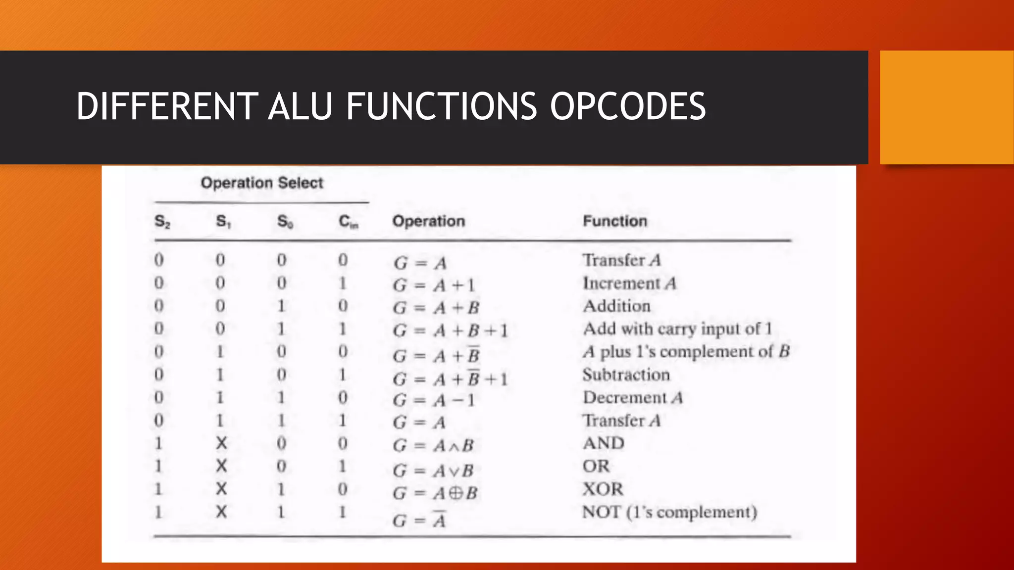
![Arithmetic Logic Unit OpCode [3:0] INST[13:10] A[15:0] ALU_Out [15:0] B[15:0] • Two 16 Bit Data inputs (Input A , Input B) • 4 Bit OpCode(Select lines) To choose A desired Function • In Our design we have 8 arithmetic operations & Four Logical Operations. • One 16 bit ALU output. • In Our Design the OpCode Holds the [13:10] bits of the instruction. module AL_Unit (OpCode , A , B , ALU_Out ) ; input [15 : 0] A , B ; input [3 : 0] OpCode ; output [15 : 0] ALU_Out ;](https://image.slidesharecdn.com/projectpresentation-150201054124-conversion-gate02/75/Controller-Implementation-in-Verilog-5-2048.jpg)
![Register File A address A_A[2:0] iNST[4:6] • Two Read Adresses To Read the Data From two Loctions in the registerfile • A_Out and B_Out are the output data selected by their addresses. • Write enable(W_E) is used to write Data on the location selected by Destination Adress(D_A). module REGISTER_FILE ( Reset , Clk , A_A , A_B , A_Out , B_Out , W_E, D_A , D_Input); input Reset, Clk; input [ 2:0] A_A, A_B; input W_E; input [ 2:0] D_A; input [15:0] D_Input; output [15:0] A_Out,B_Out; D-addres A_B[2:0] iNST[7:9] Wrie enable iNST[0] B address A_B[2:0] iNST[4:6]](https://image.slidesharecdn.com/projectpresentation-150201054124-conversion-gate02/75/Controller-Implementation-in-Verilog-7-2048.jpg)
![Control Unit • Contol Unit decodes the instruction From the Program Memory and Provides signals to the Other components. Its execution consists of three steps. 1. Fetching 2. Decoding 3. Loading module CONTROL(Clk,Reset,INST_IN,COUNT_ADD,AD_A,AD_B,AD_D,OP_CODE,W_E); input [15:0]INST_IN; input Clk,Reset ; output W_E; output [3:0] COUNT_ADD ; output [3:0] OP_CODE ; output [2:0] AD_A, AD_B, AD_D ;](https://image.slidesharecdn.com/projectpresentation-150201054124-conversion-gate02/75/Controller-Implementation-in-Verilog-10-2048.jpg)
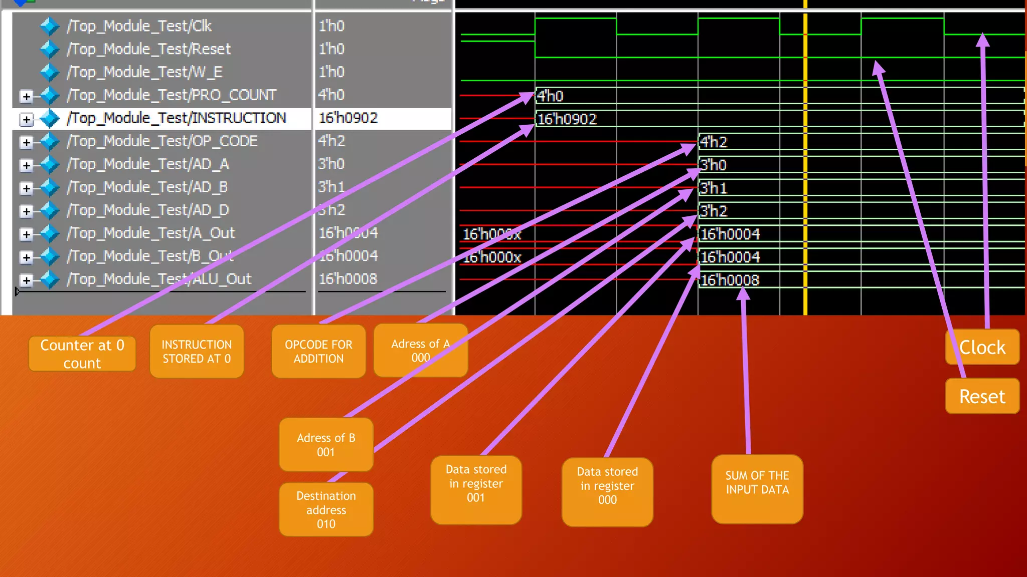
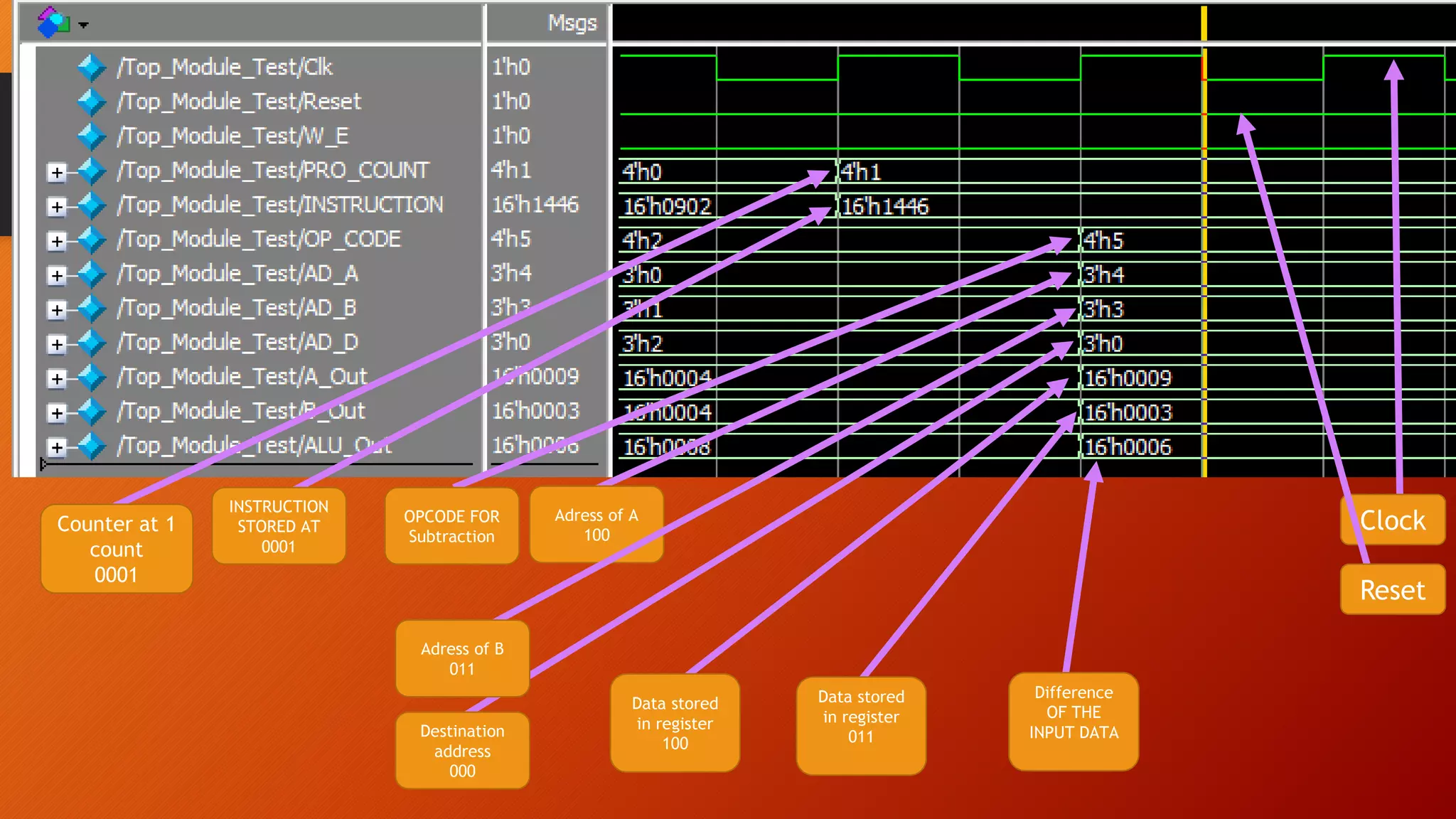
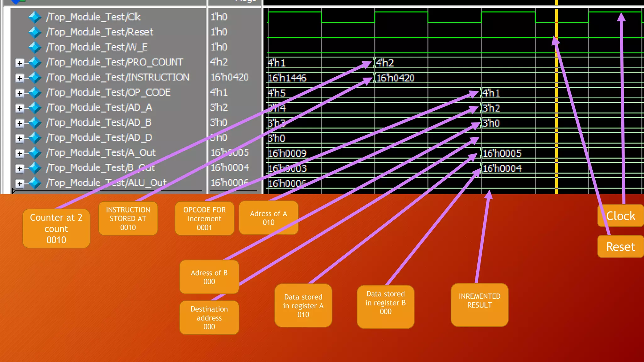
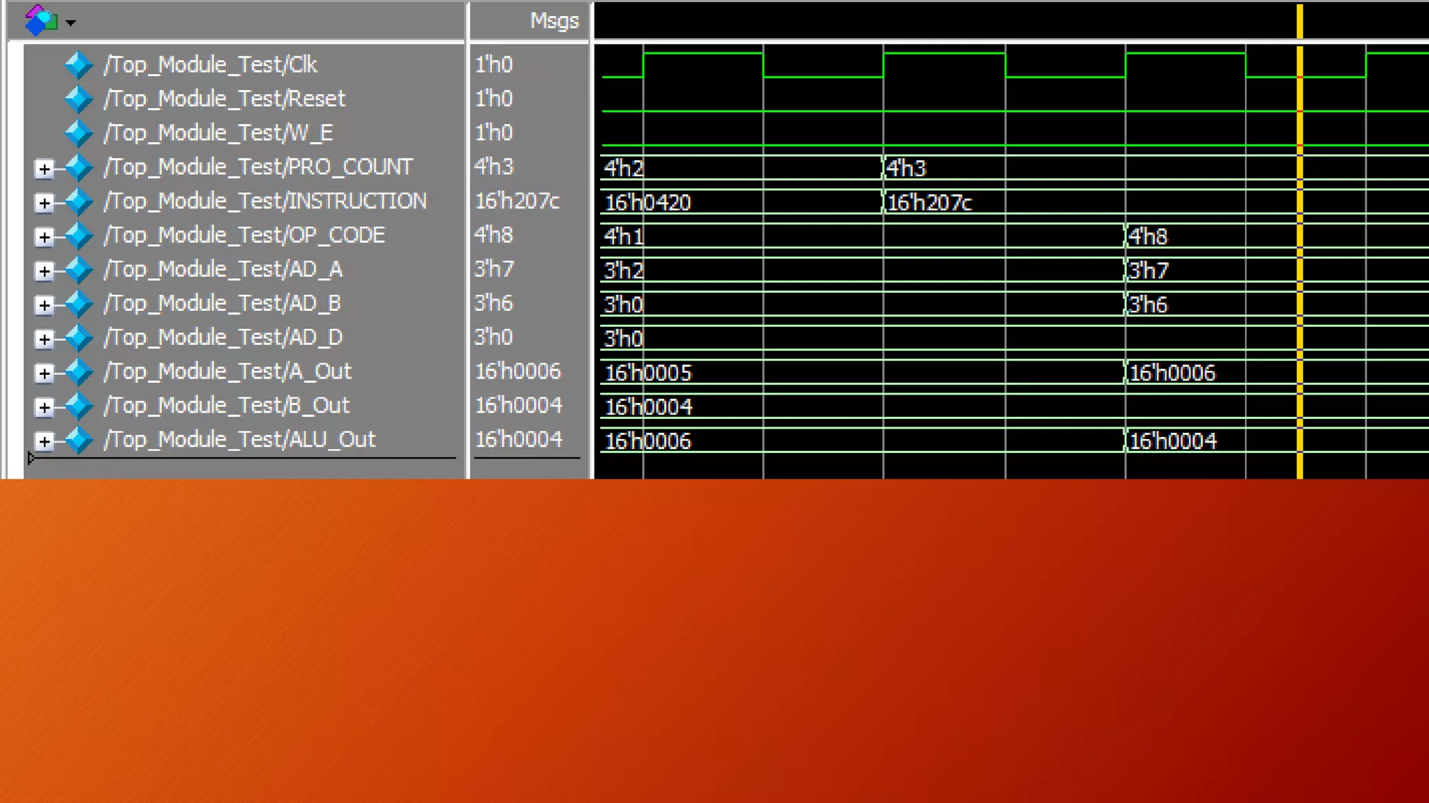

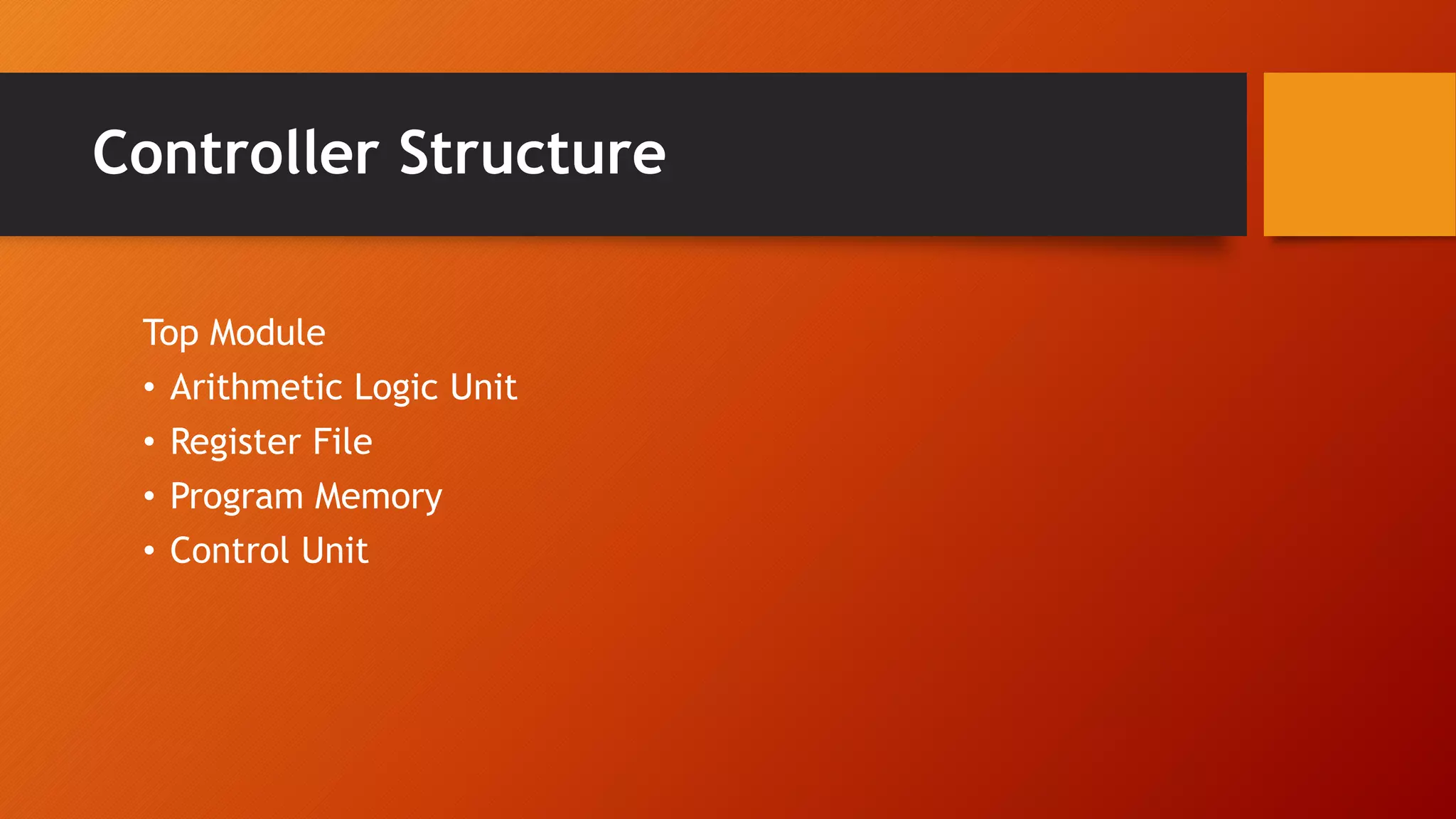
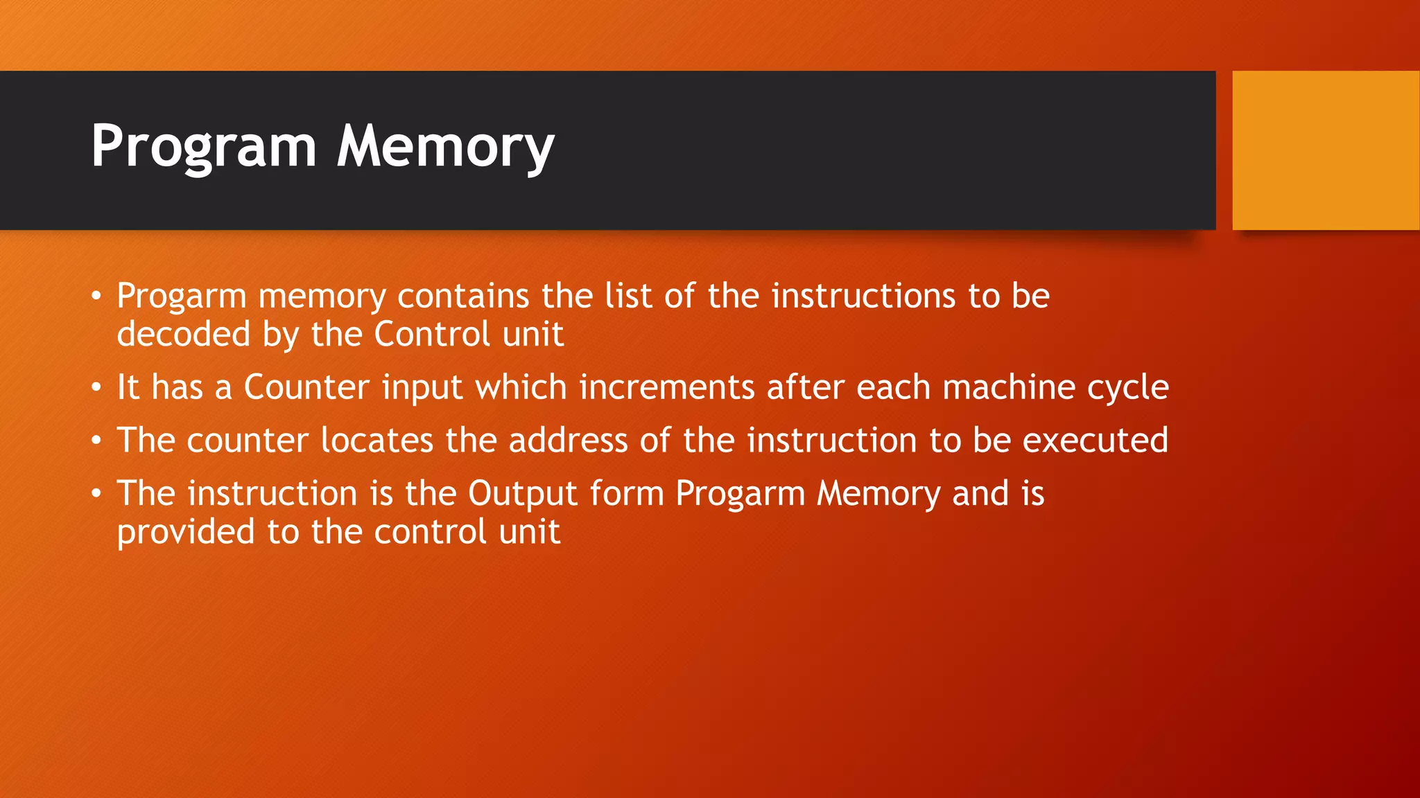
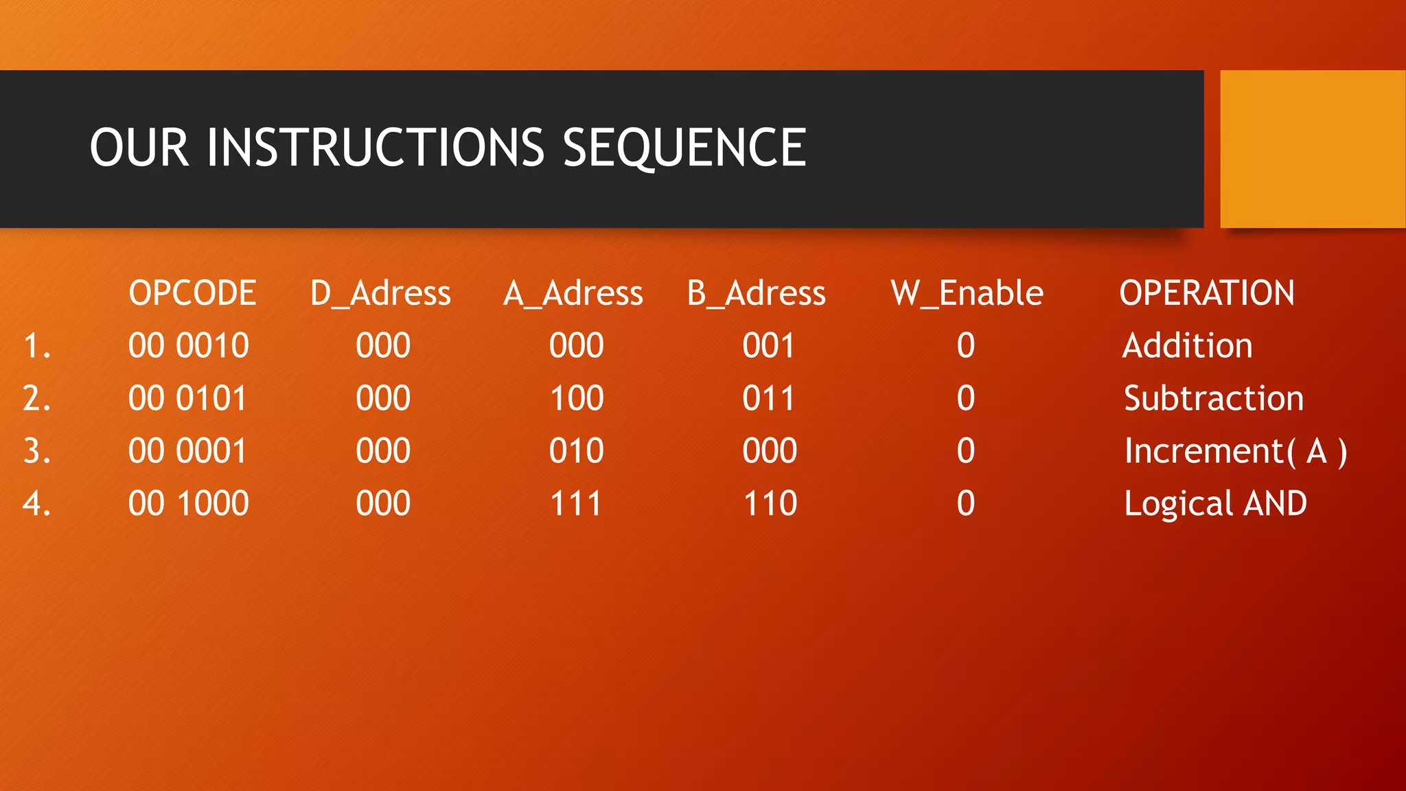
The document describes the structure and components of a controller, including: 1. The top module contains an arithmetic logic unit (ALU), register file, program memory, and control unit. 2. The ALU performs arithmetic and logical operations on two 16-bit inputs based on a 4-bit opcode. 3. The register file contains data that can be read from or written to by 3-bit addresses and a write enable signal. 4. The program memory stores instructions that are fetched and decoded by the control unit to provide control signals to other components.