The document describes the design of an encoder-decoder system in Verilog. It includes a 4-to-2 encoder, 2-to-4 decoder, and a top-level module that instantiates the encoder and decoder. The encoder and decoder are designed based on their truth tables. Verilog code and RTL schematics are provided for the encoder, decoder, and top-level modules. A full testbench and waveform are also included to test the system.
In this document
Powered by AI
Overview of the presentation by Gookyi Dennis A. N. at Hanbat National University about Encoder-Decoder in Verilog.
Outline of presentation topics including objectives, encoder, decoder, and encoder-decoder.
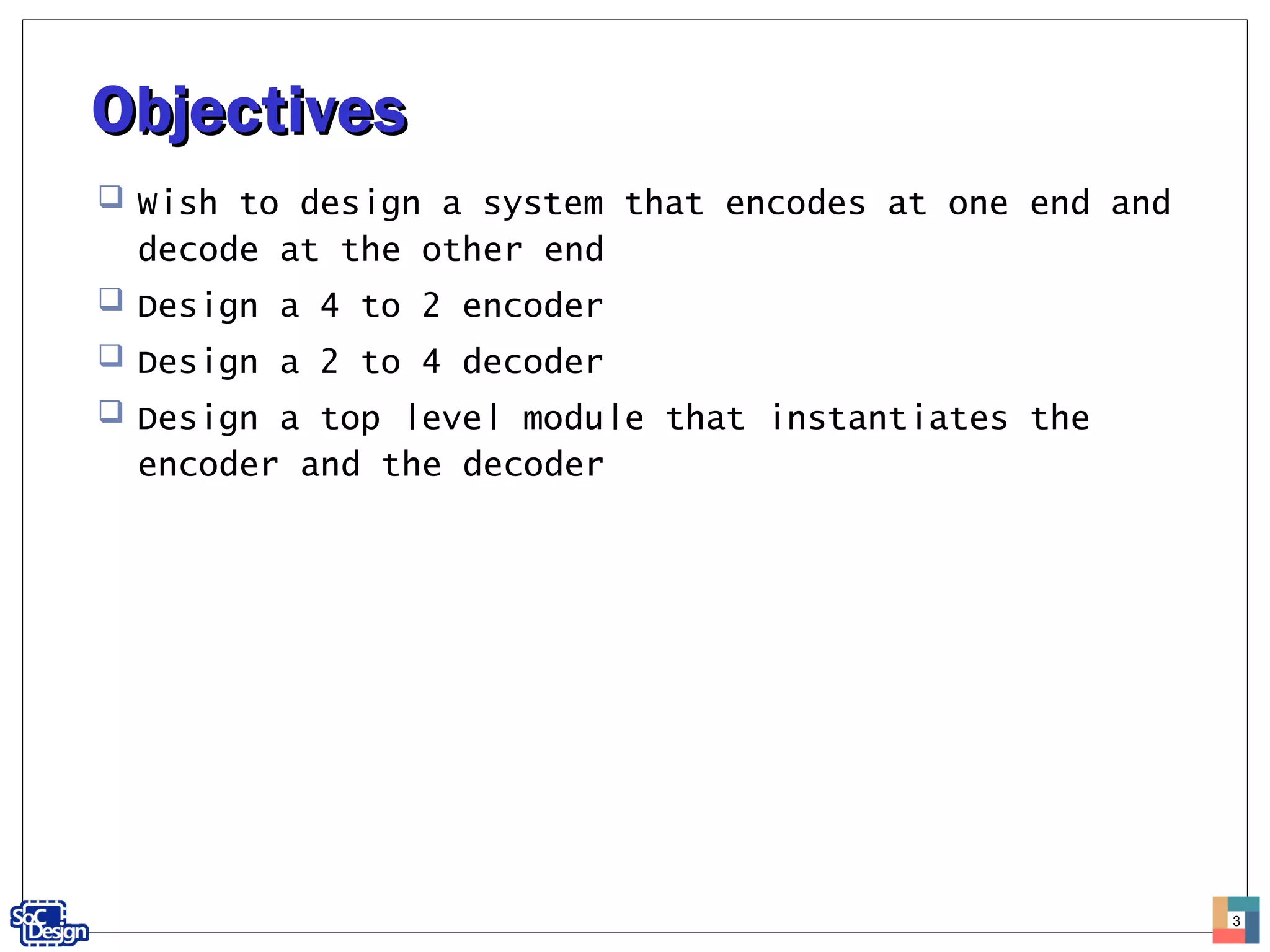
Goals to design a 4 to 2 encoder, a 2 to 4 decoder, and a top level module integrating both.
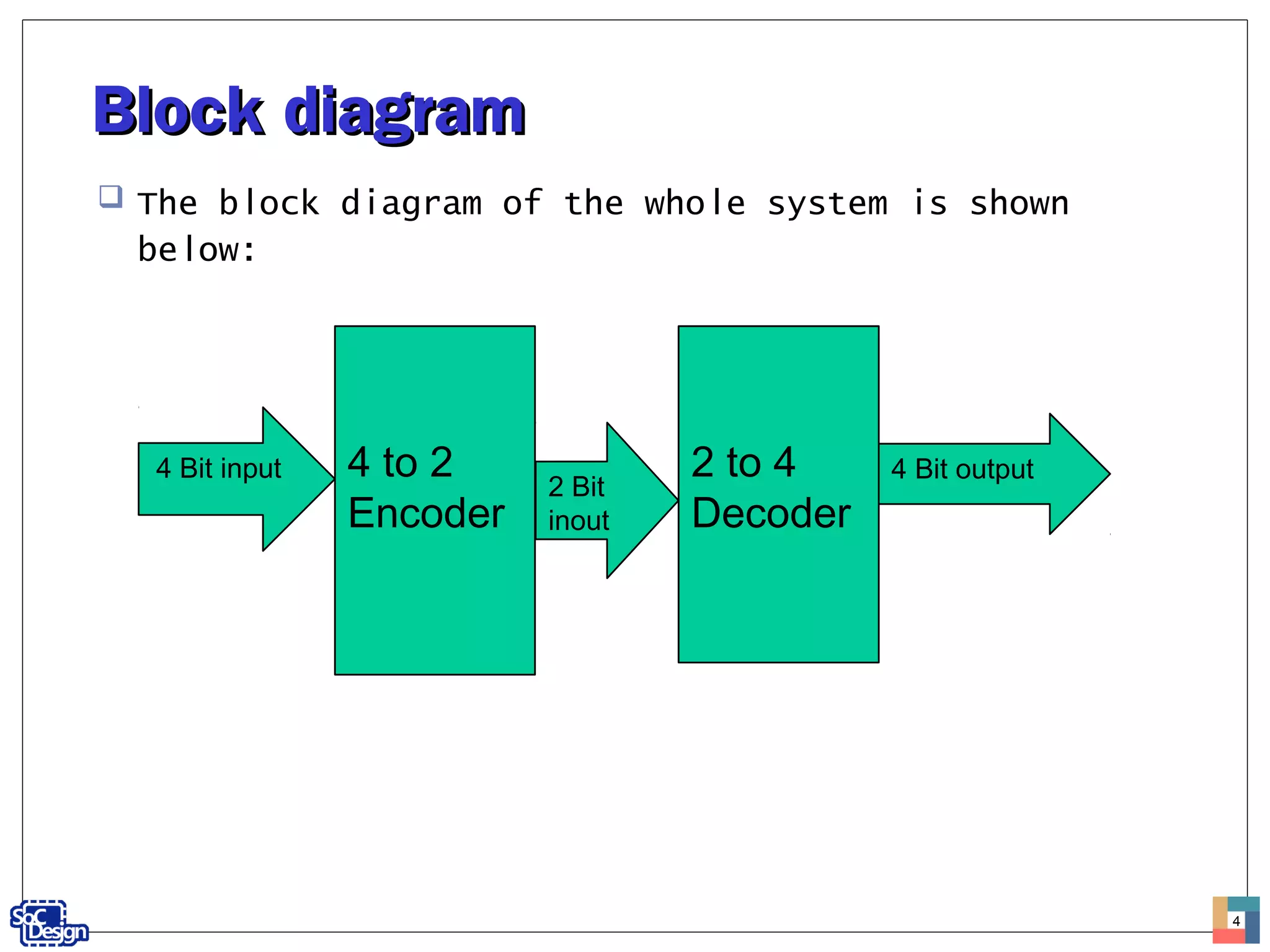
Block diagram presenting the system layout with components of a 4 to 2 encoder and a 2 to 4 decoder.
Truth table for the 4 to 2 encoder showing input-output relationships and equations.
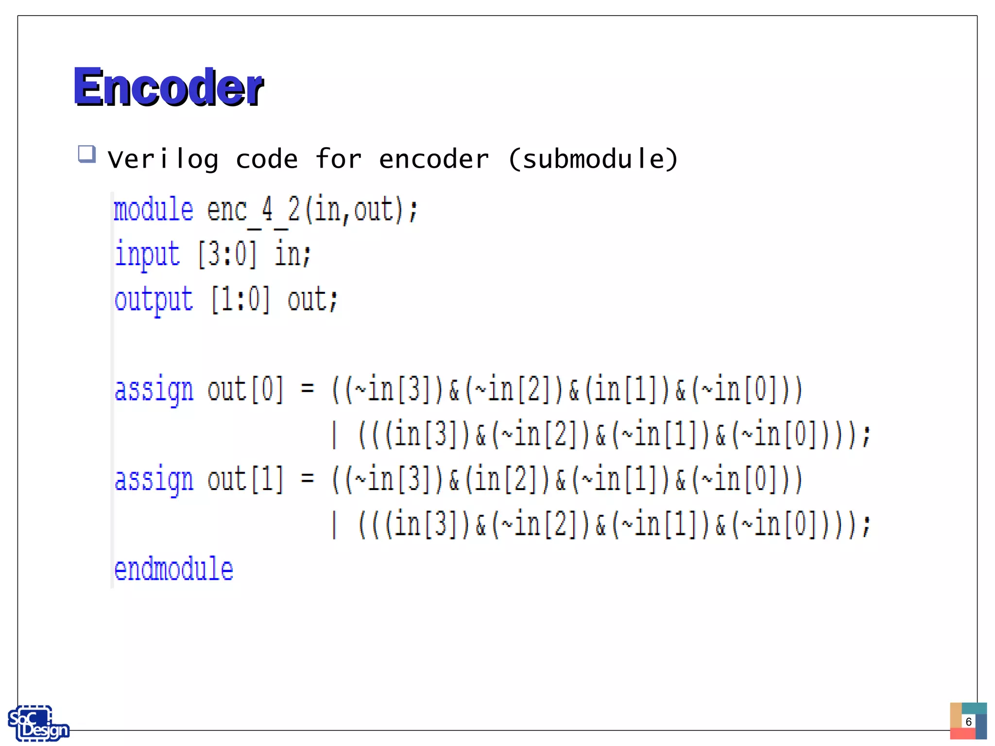
Presentation of the Verilog code developed for the encoder submodule.
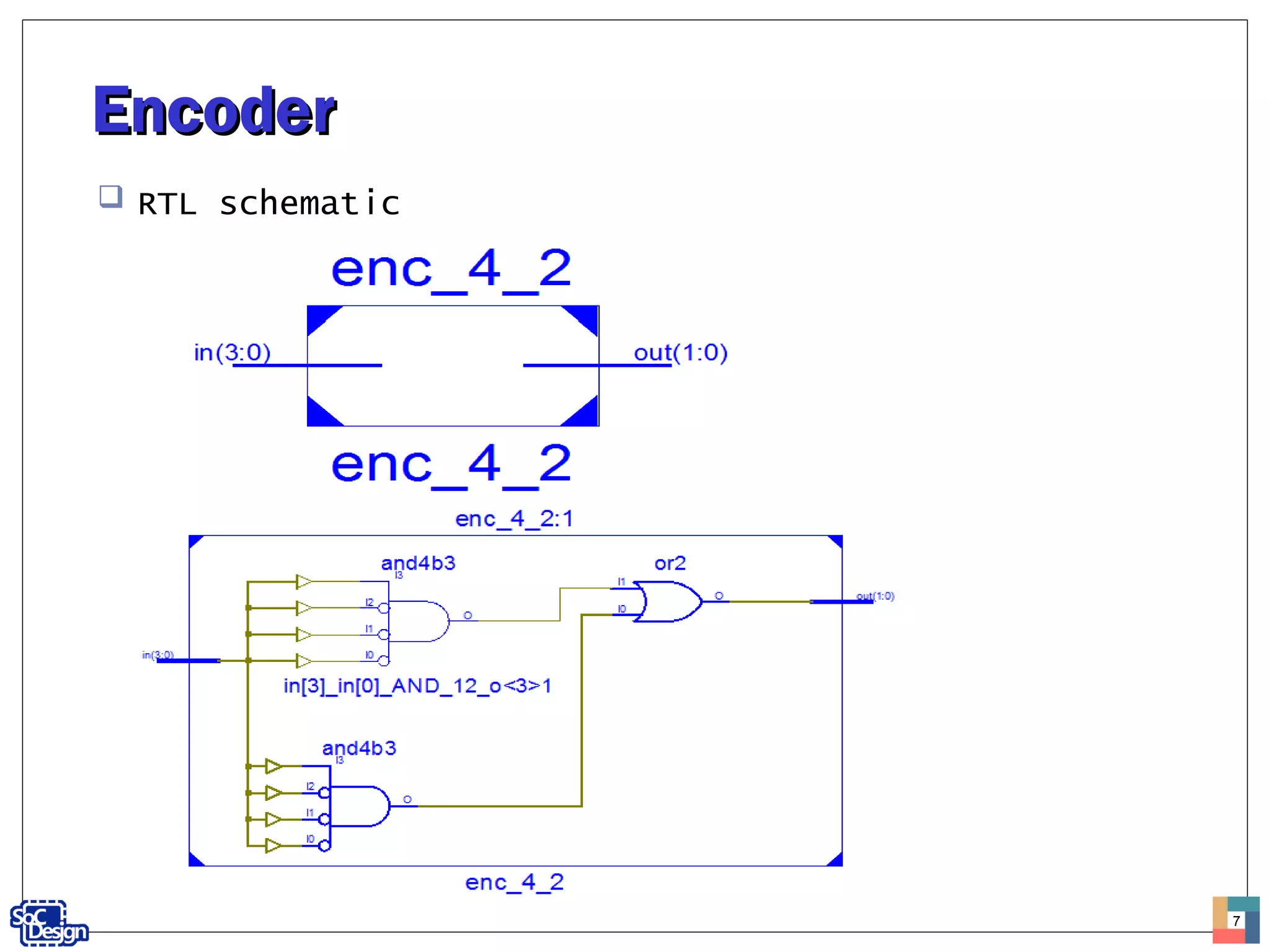
Representation of the Encoder in RTL schematic format.
Truth table for the 2 to 4 decoder displaying output equations and configurations.
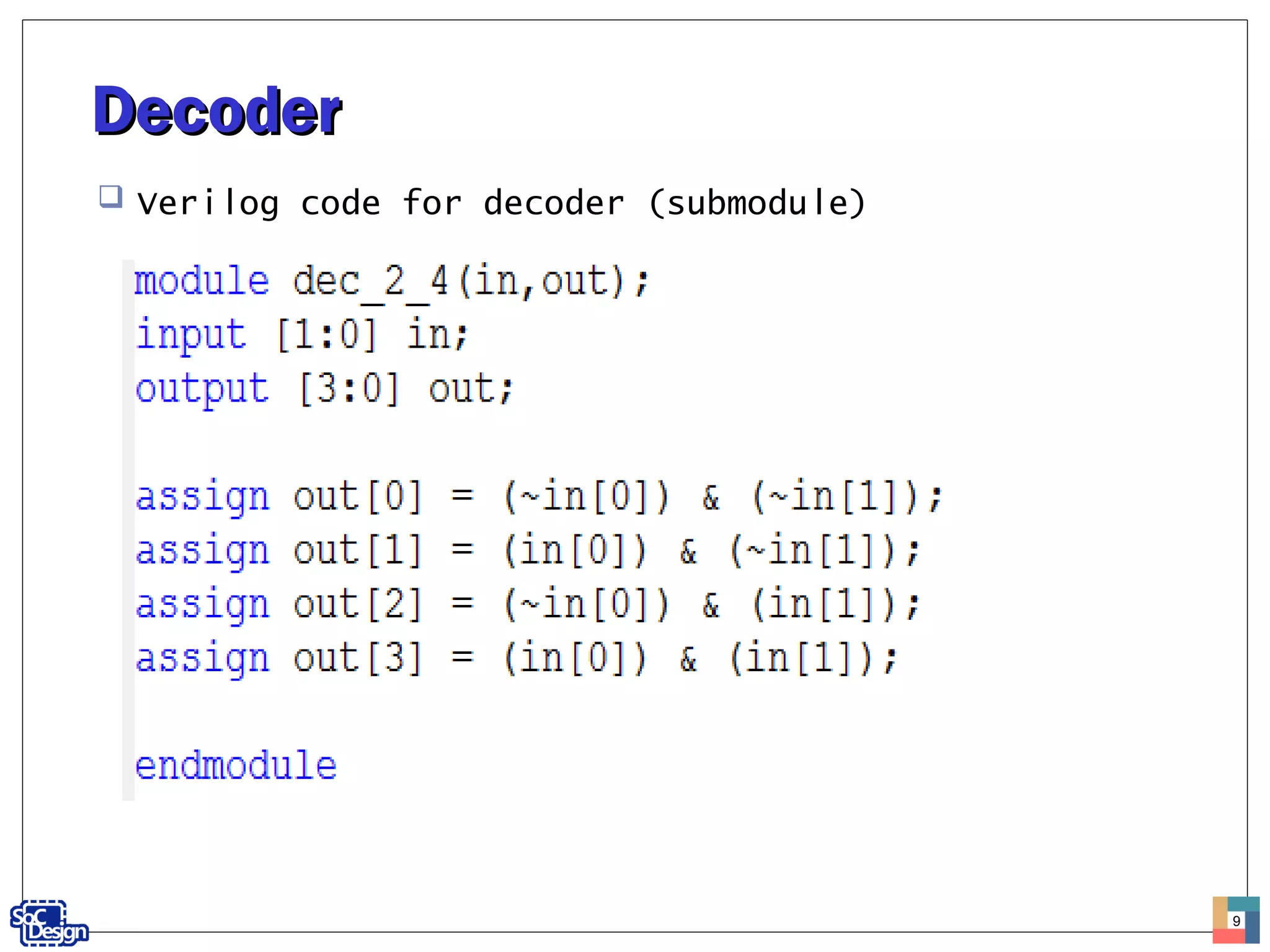
Demonstration of the Verilog code for the decoder submodule.
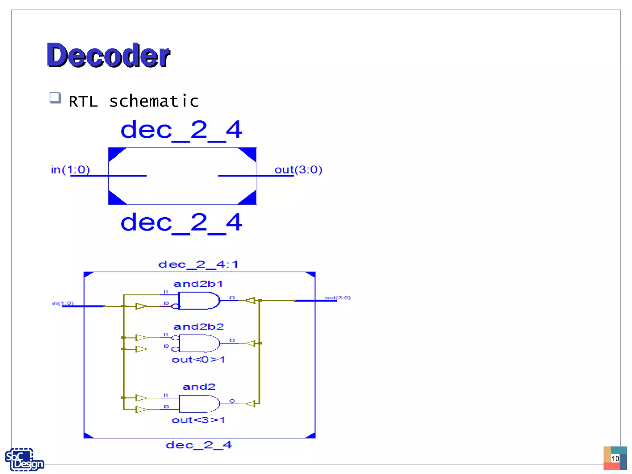
Visual depiction of the Decoder in RTL schematic format.
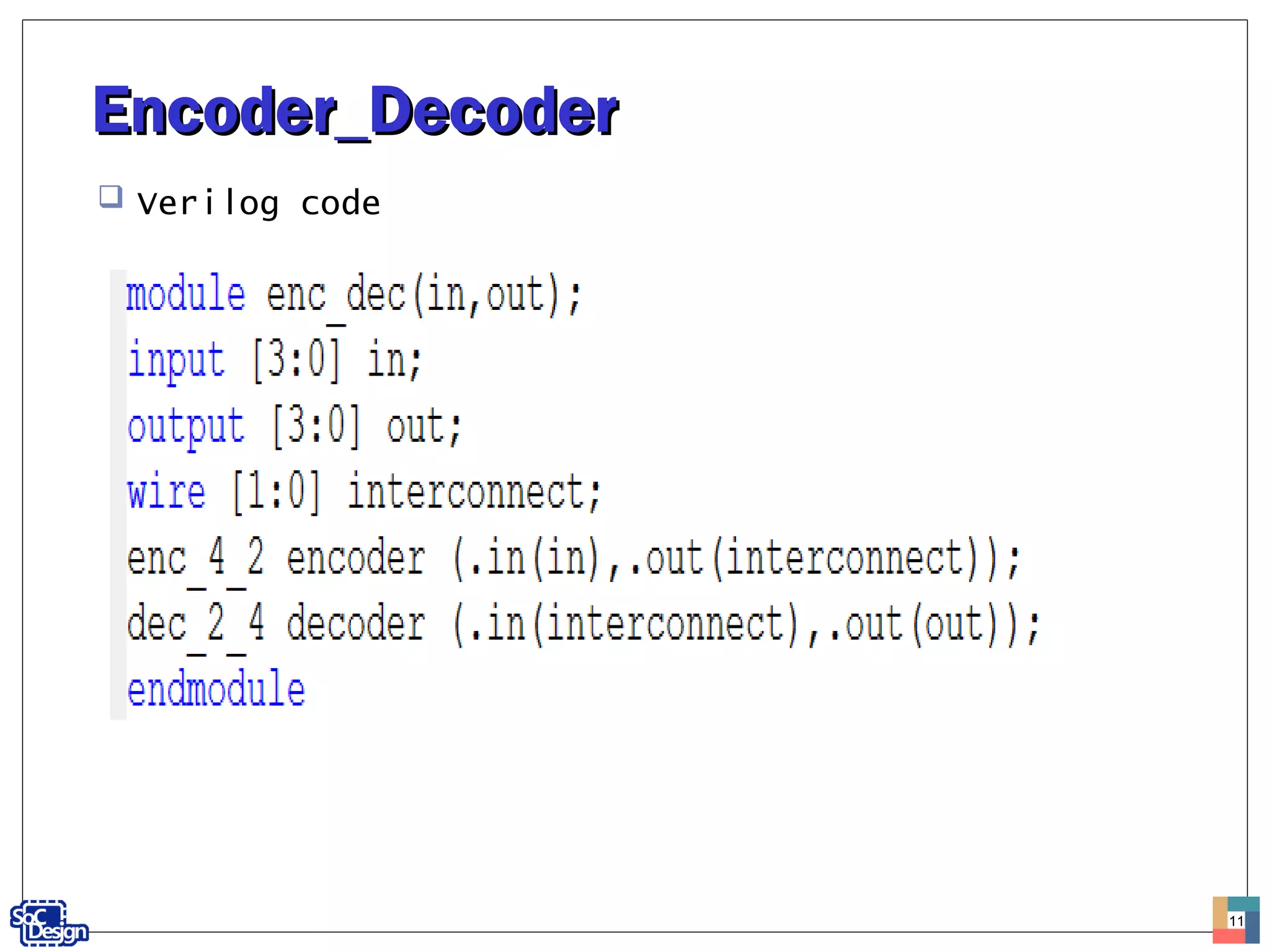
The Verilog code for the combined Encoder-Decoder system.
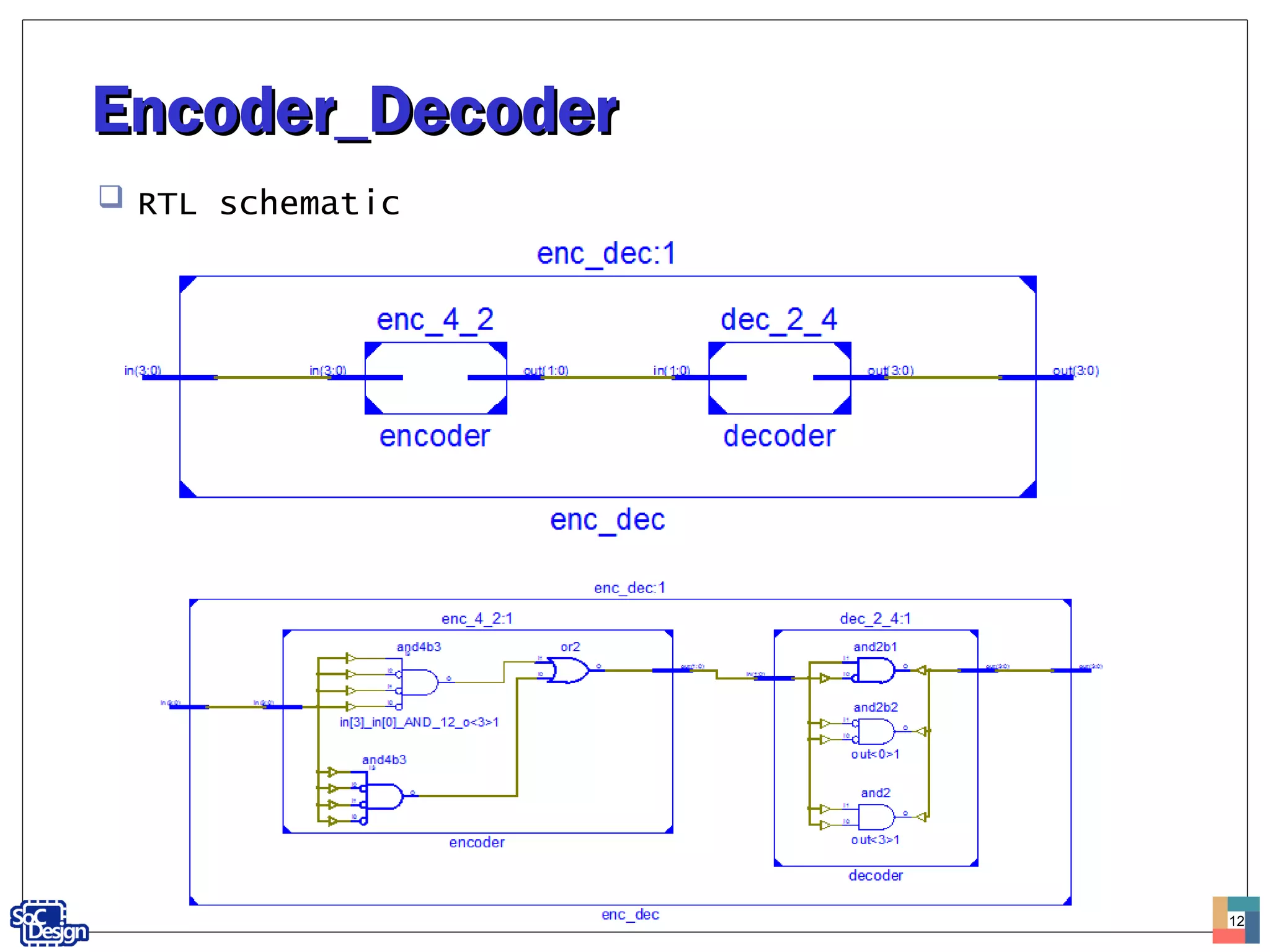
RTL schematic representation for the complete Encoder-Decoder system.
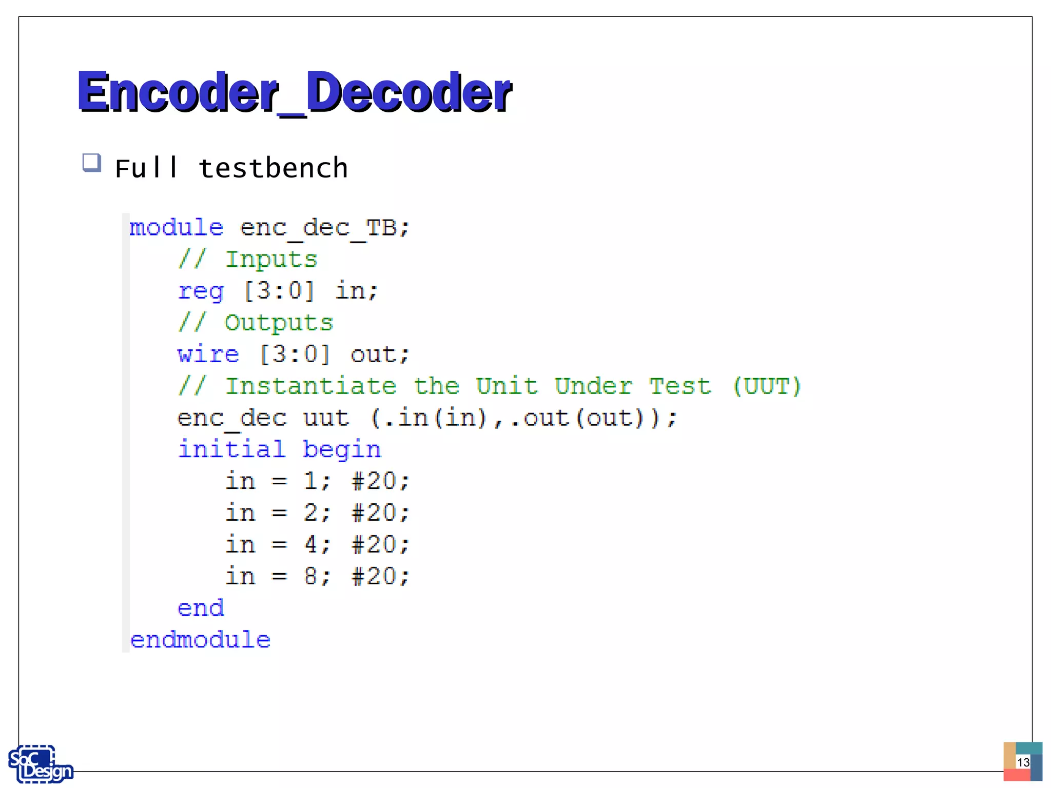
Comprehensive testbench code to validate the Encoder-Decoder functionality.
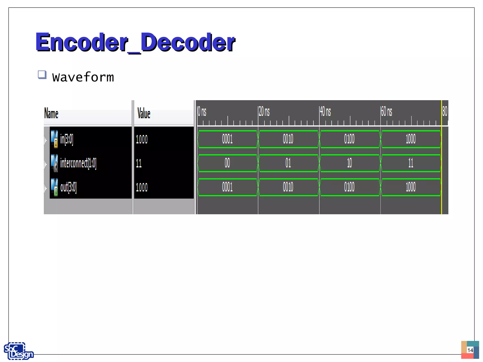
Presentation of waveform outputs demonstrating the performance of the Encoder-Decoder system.
ObjectivesObjectives Wish todesign a system that encodes at one end and decode at the other end Design a 4 to 2 encoder Design a 2 to 4 decoder Design a top level module that instantiates the encoder and the decoder 3
4.
Block diagramBlock diagram The block diagram of the whole system is shown below: 4 4 to 2 Encoder 2 to 4 Decoder 4 Bit input 4 Bit output 2 Bit inout
![EncoderEncoder Truth table of 4 to 2 encoder is shown below: Output equations are as follows: out[0] = ((~in[3])&(~in[2])&(in[1])&(~in[0])) | (((in[3])&(~in[2])&(~in[1])&(~in[0])))out[0] = ((~in[3])&(~in[2])&(in[1])&(~in[0])) | (((in[3])&(~in[2])&(~in[1])&(~in[0]))) out[1] = ((~in[3])&(in[2])&(~in[1])&(~in[0])) | (((in[3])&(~in[2])&(~in[1])&(~in[0])))out[1] = ((~in[3])&(in[2])&(~in[1])&(~in[0])) | (((in[3])&(~in[2])&(~in[1])&(~in[0]))) 5 In[3] In[2] In[1] In[0] Out[1] Out[0] 0 0 0 1 0 0 0 0 1 0 0 1 0 1 0 0 1 0 1 0 0 0 1 1](https://image.slidesharecdn.com/encoderdecoder-140718051244-phpapp02/75/Encoder-decoder-5-2048.jpg)
![DecoderDecoder Truth table for 2 to 4 decoder Output equations are as follows: out[0] = (~in[0]) & (~in[1]) out[1] = (in[0]) & (~in[1]) out[2] = (~in[0]) & (in[1]) out[3] = (in[0]) & (in[1]) 8 In[1] In[0] Out[3] Out[2] Out[1] Out[0] 0 0 0 0 0 1 0 1 0 0 1 0 1 0 0 1 0 0 1 0 1 0 0 0](https://image.slidesharecdn.com/encoderdecoder-140718051244-phpapp02/75/Encoder-decoder-8-2048.jpg)