MICROCONTROLLER MODULE-1 PPT Includes basics of microcontroller , applications,memory interfacing etc...
1.
ANJUMAN INSTITUTE OFTECHNOLOGY AND MANAGEMENT BHATKAL-581320 DEPARTMENT OF ELECTRONICS AND COMMUNICATION ENGINEERING MODULE-1 MICROCONTROLLER
2.
TEXT BOOKS 1)“The 8051Microcontroller and Embedded Systems – using Assembly and C”, Muhammad Ali Mazidi and Janice Gillespie Mazidi and Rollin D. McKinlay ; PHI, 2006/Pearson, 2006. 2)“The 8051 Microcontroller”, Kenneth J. Ayala, 3rd Edition, Thomson /Cengage Learning. 3)“Programming and customizing the 8051 Microcontroller”, Myke Predko Tata Mc Graw-Hill Edition 1999. REFERENCE BOOKS 1)“The 8051 Microcontroller based Embedded Systems”, Manish K Patel, McGraw Hill, 2014, ISBN : 978-93-329-0125-4. 2)“Microcontrollers : Architecture, Programming, Interfacing and System Design”, Raj Kamal, Pearson Education, 2005.
CONTENTS • Microcontrollers • Historyof 8051 Microcontroller • Applications of Microcontrollers • Types of microcontrollers • Microprocessor Vs Microcontrollers • Computer Architecture / Processor Architecture • Features of Microcontroller • 8051 Pin diagram • 8051 Architecture
5.
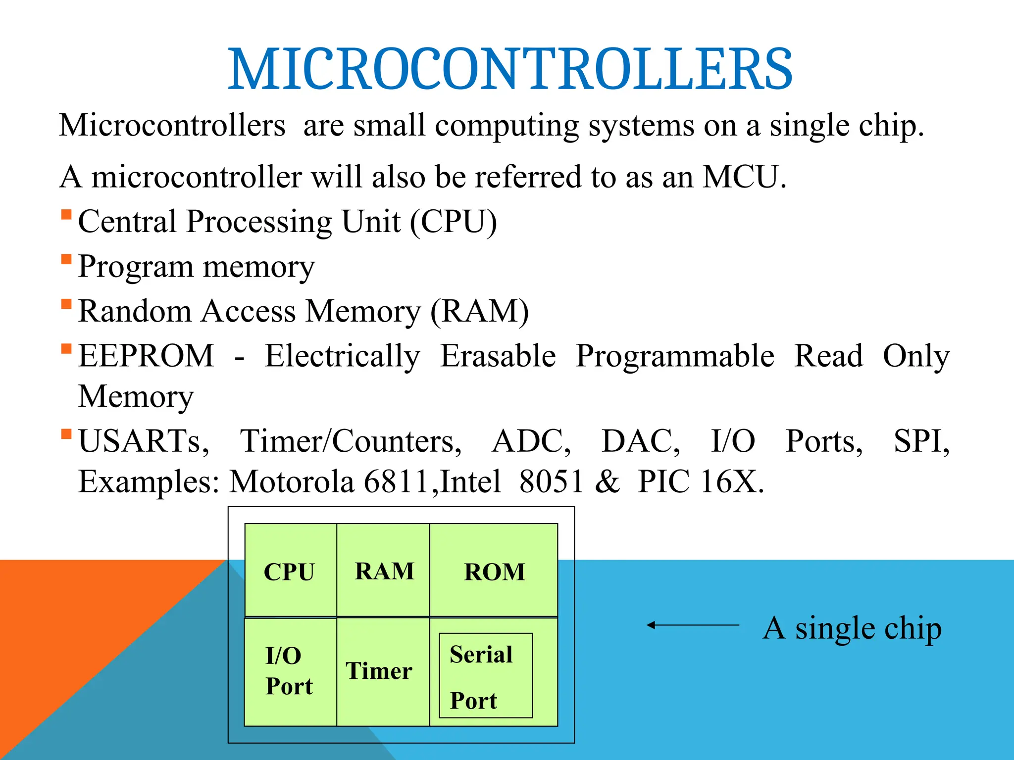
MICROCONTROLLERS Microcontrollers are smallcomputing systems on a single chip. A microcontroller will also be referred to as an MCU. Central Processing Unit (CPU) Program memory Random Access Memory (RAM) EEPROM - Electrically Erasable Programmable Read Only Memory USARTs, Timer/Counters, ADC, DAC, I/O Ports, SPI, Examples: Motorola 6811,Intel 8051 & PIC 16X. CPU RAM ROM I/O Port Timer Serial Port A single chip
6.
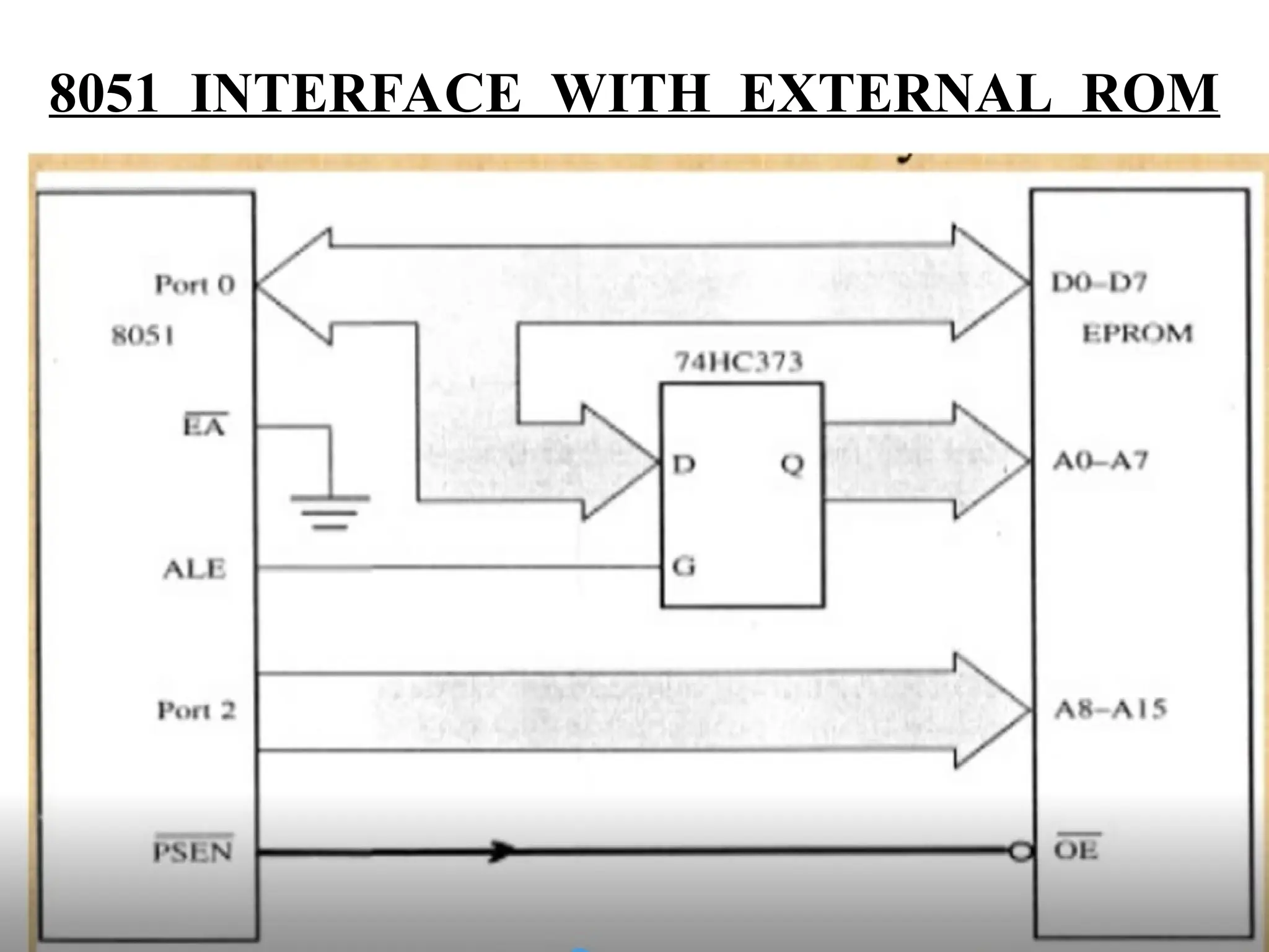
HISTORY OF 8051MICROCONTROLLER • In the year 1980 Intel Corporation introduced an 8 bit microcontroller called 8051. • It has 4K bytes of ROM,128 Bytes of RAM , a serial port, two 16-bit Timers and 32 I/O pins. • CPU can work with 8 bit of data at a time. • Data larger than 8 bit can be broken into 8 bit size to be processed by the CPU.
7.
APPLICATIONS OF MICROCONTROLLERS •Cell phone • Watch • Calculator • Video Games • Alarm clock • Air Conditioner • TV remote • Microwave Oven • Washing Machines • Robotic System • Anti-Lock Braking System Monitor
8.
TYPES OF MICROCONTROLLERS •Based on bits 1) 4-bit (Eg: Renasas M34501 with 20 pin DIP) 2) 8-bit (Eg: 8031, 8051 microcontroller) 3) 16-bit (Eg: 8096 microcontroller, Motorola 68HC16Z3) 4) 32-bit (Eg: Intel 80960, Motorola M683XX, Intel/Atmel 251 family microcontroller) • Based on memory 1) External memory – built-in memories are not useful so connected to external memory by the help of parallel port pins. Eg: Intel 8031 2) Embedded memory- Program, data memory, I/O ports, Timers/Counters are on same chip. Eg :8051 microcontroller • Based on Instruction set 1) CISC – Single instruction can perform many operations 2) RISC – Different instructions perform different operations
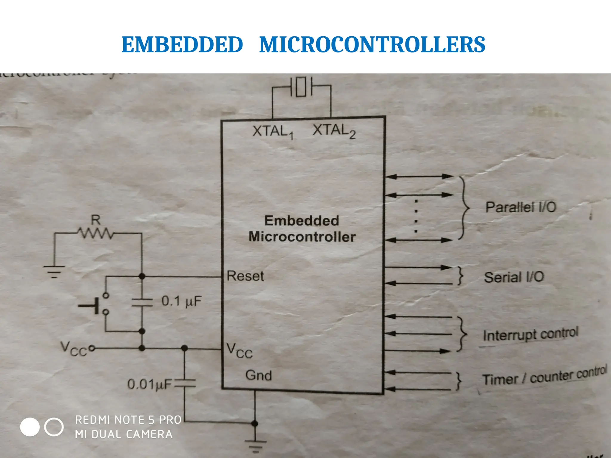
• When acomplete hardware required to run a particular application is provided on the microcontroller chip, it is referred to as an embedded microcontroller. • Embedded microcontrollers only require power, reset circuit and clock. • Embedded microcontrollers communicate with external devices with its digital input output pins.
12.
CRITERIA FOR SELECTINGMICROCONTROLLER • Speed • Packaging • Power consumption • Amount of RAM, ROM on chip • Number of I/0 pins and the timer on chip • Cost per unit • Availability of software development tools such as compilers, assemblers and debuggers
13.
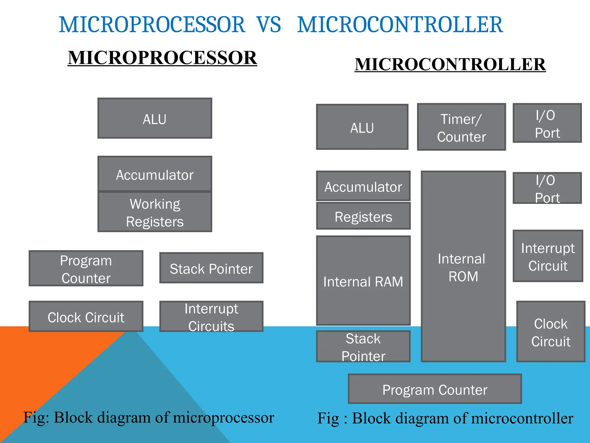
MICROPROCESSOR VS MICROCONTROLLER MICROPROCESSORMICROCONTROLLER ALU Accumulator Working Registers Program Counter Stack Pointer Clock Circuit Interrupt Circuits Fig: Block diagram of microprocessor ALU Accumulator Registers Timer/ Counter Stack Pointer Internal ROM Program Counter I/O Port I/O Port Interrupt Circuit Clock Circuit Fig : Block diagram of microcontroller Internal RAM
14.
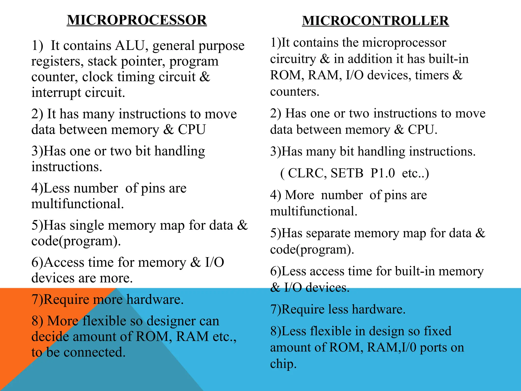
MICROPROCESSOR 1) It containsALU, general purpose registers, stack pointer, program counter, clock timing circuit & interrupt circuit. 2) It has many instructions to move data between memory & CPU 3)Has one or two bit handling instructions. 4)Less number of pins are multifunctional. 5)Has single memory map for data & code(program). 6)Access time for memory & I/O devices are more. 7)Require more hardware. 8) More flexible so designer can decide amount of ROM, RAM etc., to be connected. MICROCONTROLLER 1)It contains the microprocessor circuitry & in addition it has built-in ROM, RAM, I/O devices, timers & counters. 2) Has one or two instructions to move data between memory & CPU. 3)Has many bit handling instructions. ( CLRC, SETB P1.0 etc..) 4) More number of pins are multifunctional. 5)Has separate memory map for data & code(program). 6)Less access time for built-in memory & I/O devices. 7)Require less hardware. 8)Less flexible in design so fixed amount of ROM, RAM,I/0 ports on chip.
15.
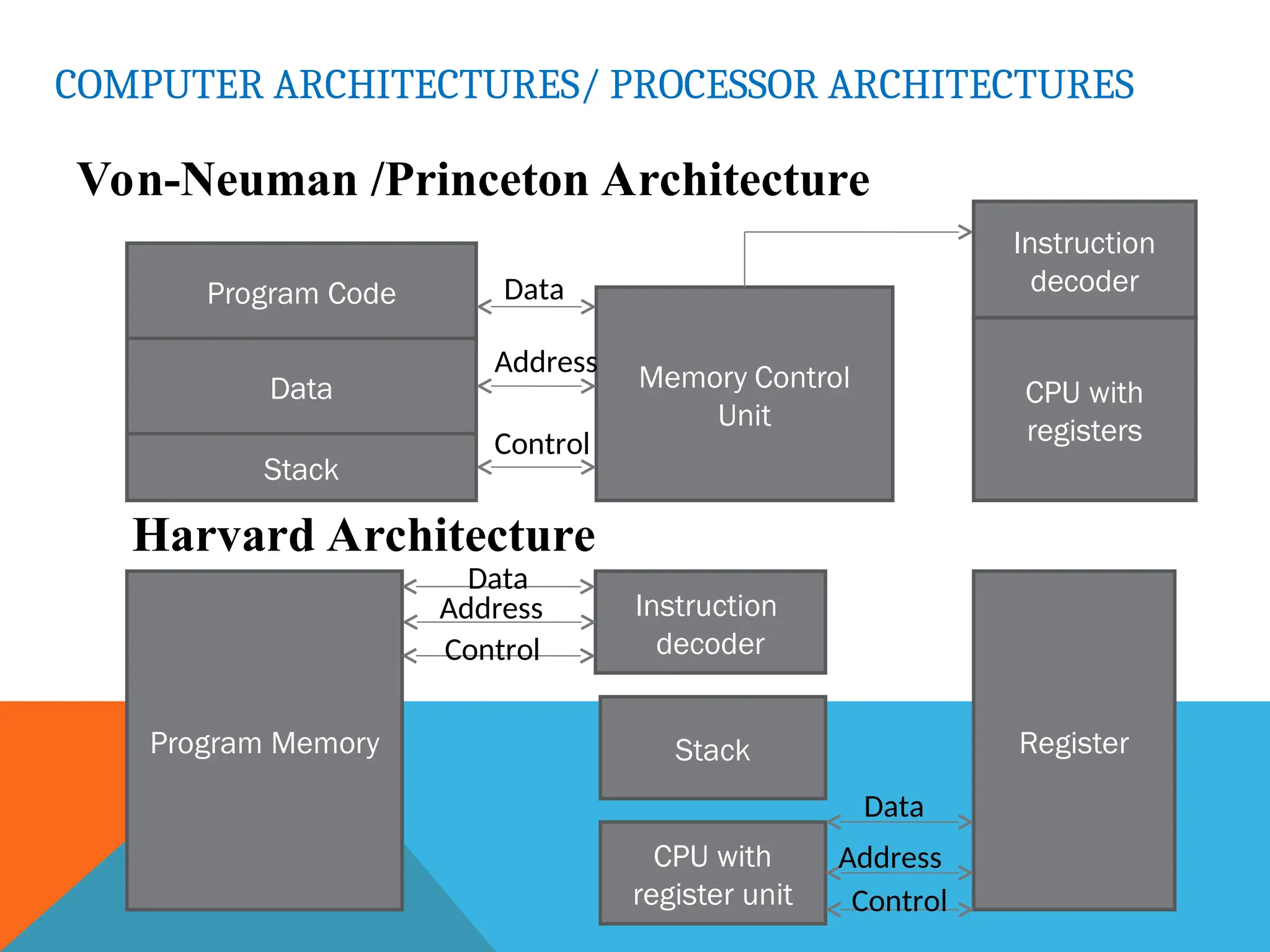
COMPUTER ARCHITECTURES/ PROCESSORARCHITECTURES Von-Neuman /Princeton Architecture Program Code Data Stack Memory Control Unit Instruction decoder CPU with registers Harvard Architecture Data Address Control Program Memory Instruction decoder Stack CPU with register unit Register Data Address Control Data Address Control
16.
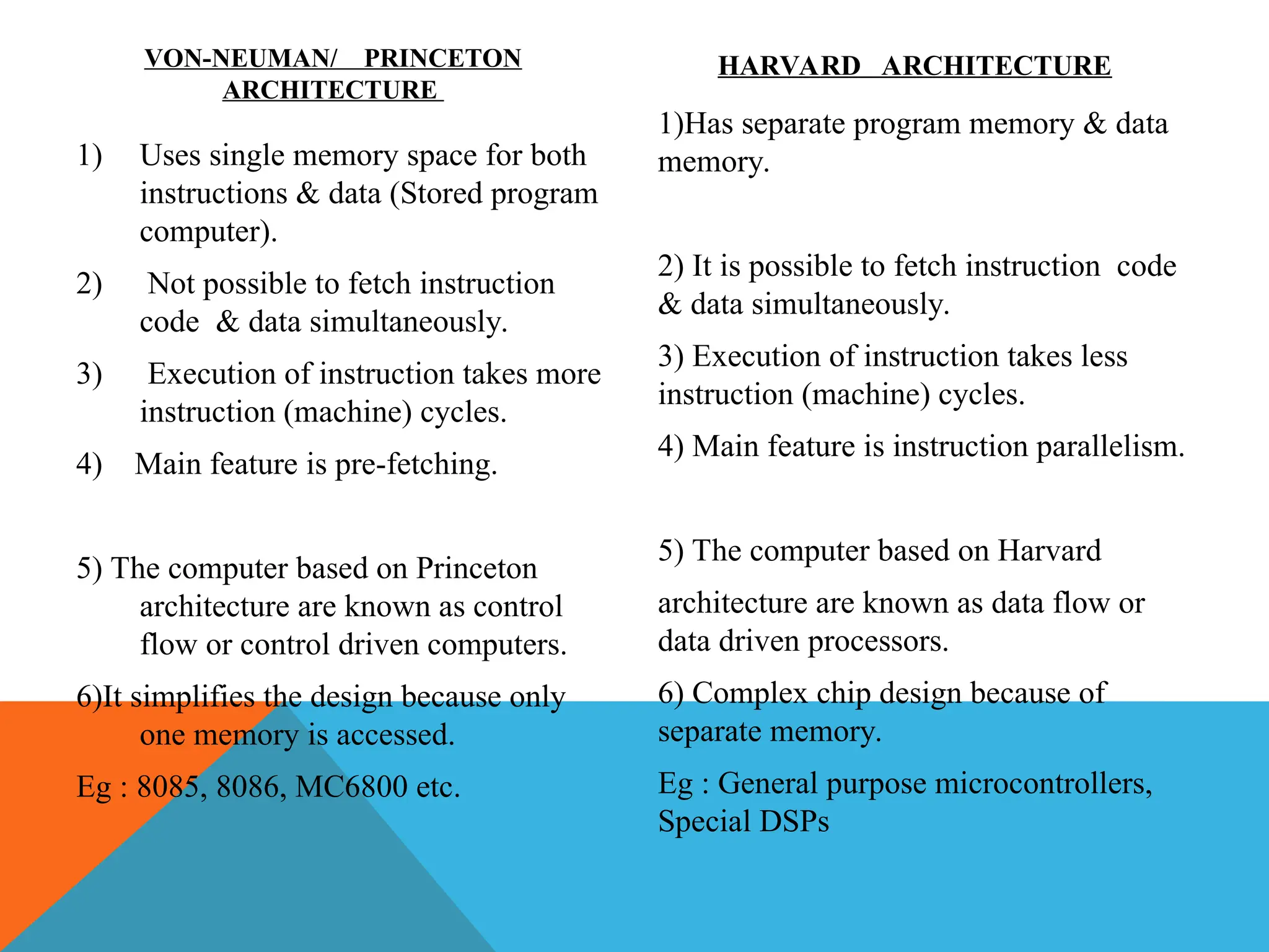
VON-NEUMAN/ PRINCETON ARCHITECTURE 1) Usessingle memory space for both instructions & data (Stored program computer). 2) Not possible to fetch instruction code & data simultaneously. 3) Execution of instruction takes more instruction (machine) cycles. 4) Main feature is pre-fetching. 5) The computer based on Princeton architecture are known as control flow or control driven computers. 6)It simplifies the design because only one memory is accessed. Eg : 8085, 8086, MC6800 etc. HARVARD ARCHITECTURE 1)Has separate program memory & data memory. 2) It is possible to fetch instruction code & data simultaneously. 3) Execution of instruction takes less instruction (machine) cycles. 4) Main feature is instruction parallelism. 5) The computer based on Harvard architecture are known as data flow or data driven processors. 6) Complex chip design because of separate memory. Eg : General purpose microcontrollers, Special DSPs
17.
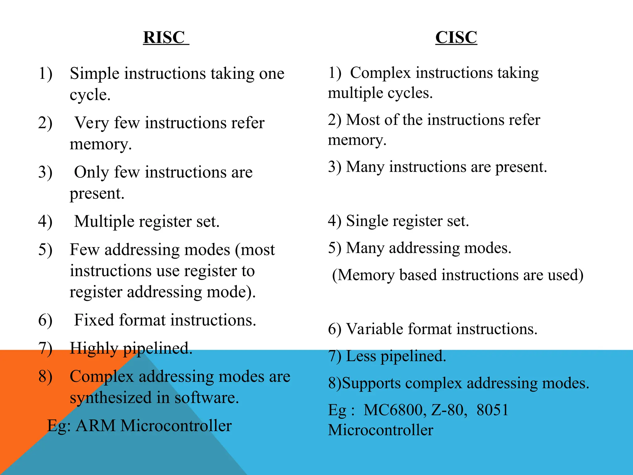
RISC 1) Simple instructionstaking one cycle. 2) Very few instructions refer memory. 3) Only few instructions are present. 4) Multiple register set. 5) Few addressing modes (most instructions use register to register addressing mode). 6) Fixed format instructions. 7) Highly pipelined. 8) Complex addressing modes are synthesized in software. Eg: ARM Microcontroller CISC 1) Complex instructions taking multiple cycles. 2) Most of the instructions refer memory. 3) Many instructions are present. 4) Single register set. 5) Many addressing modes. (Memory based instructions are used) 6) Variable format instructions. 7) Less pipelined. 8)Supports complex addressing modes. Eg : MC6800, Z-80, 8051 Microcontroller
18.
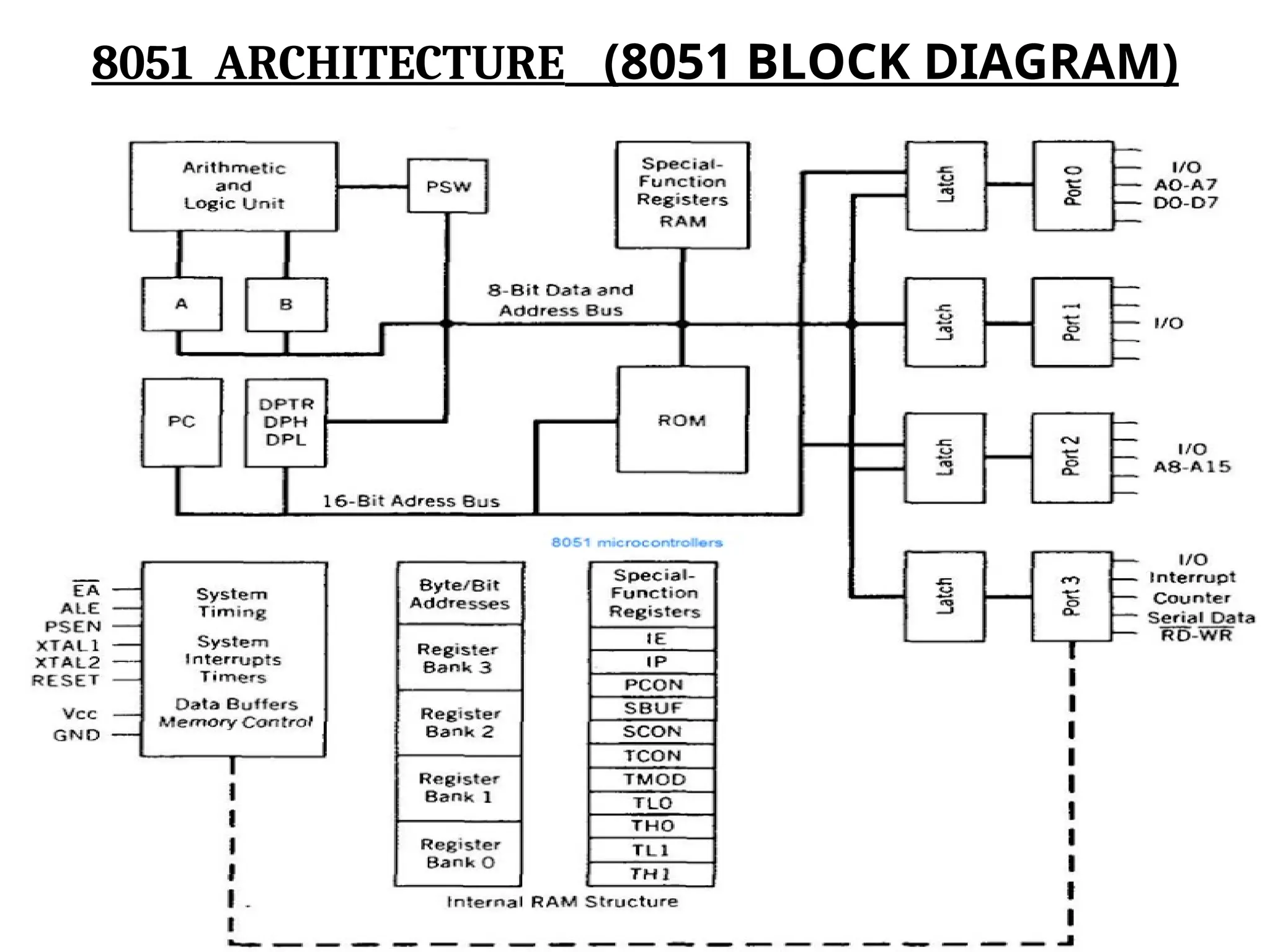
FEATURES OF 8051MICROCONTROLLER 1) 8 bit CPU 2) On chip clock oscillator 3) 4K bytes of internal program memory (code memory ) [ROM] 4) 128 bytes of internal data memory [RAM] 5) 64K bytes of external program memory address space 6) 64K bytes of external data memory space 7) 32 bidirectional I/O lines 8) Two 16 bit Timer/ Counter : T0, T1 9) Full duplex serial data receiver/ transmitter 10)Four register banks with 8 registers in each bank 11)Sixteen bit Program Counter (PC) and Data pointer(DPTR) 12)8 bit Program Status Word (PSW) and 8 bit Stack pointer 13)Two external and three internal interrupt sources
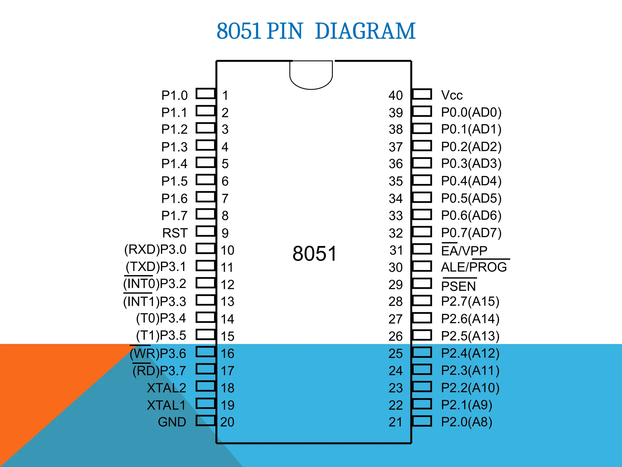
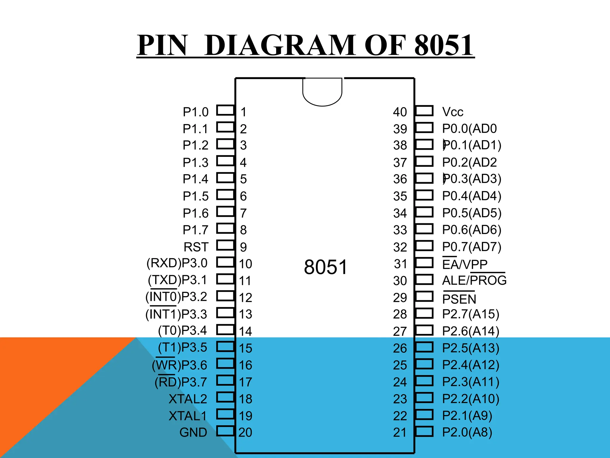
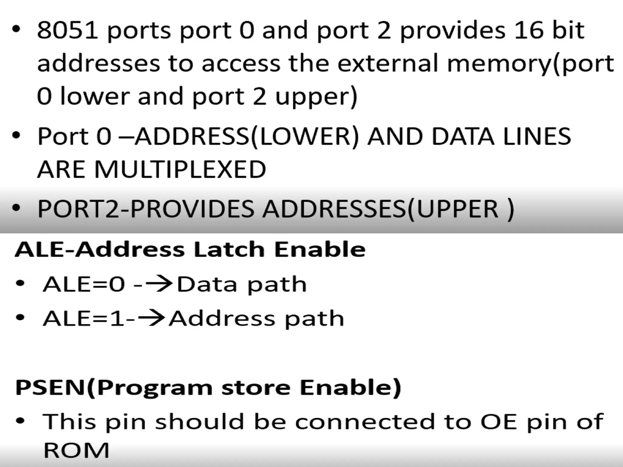
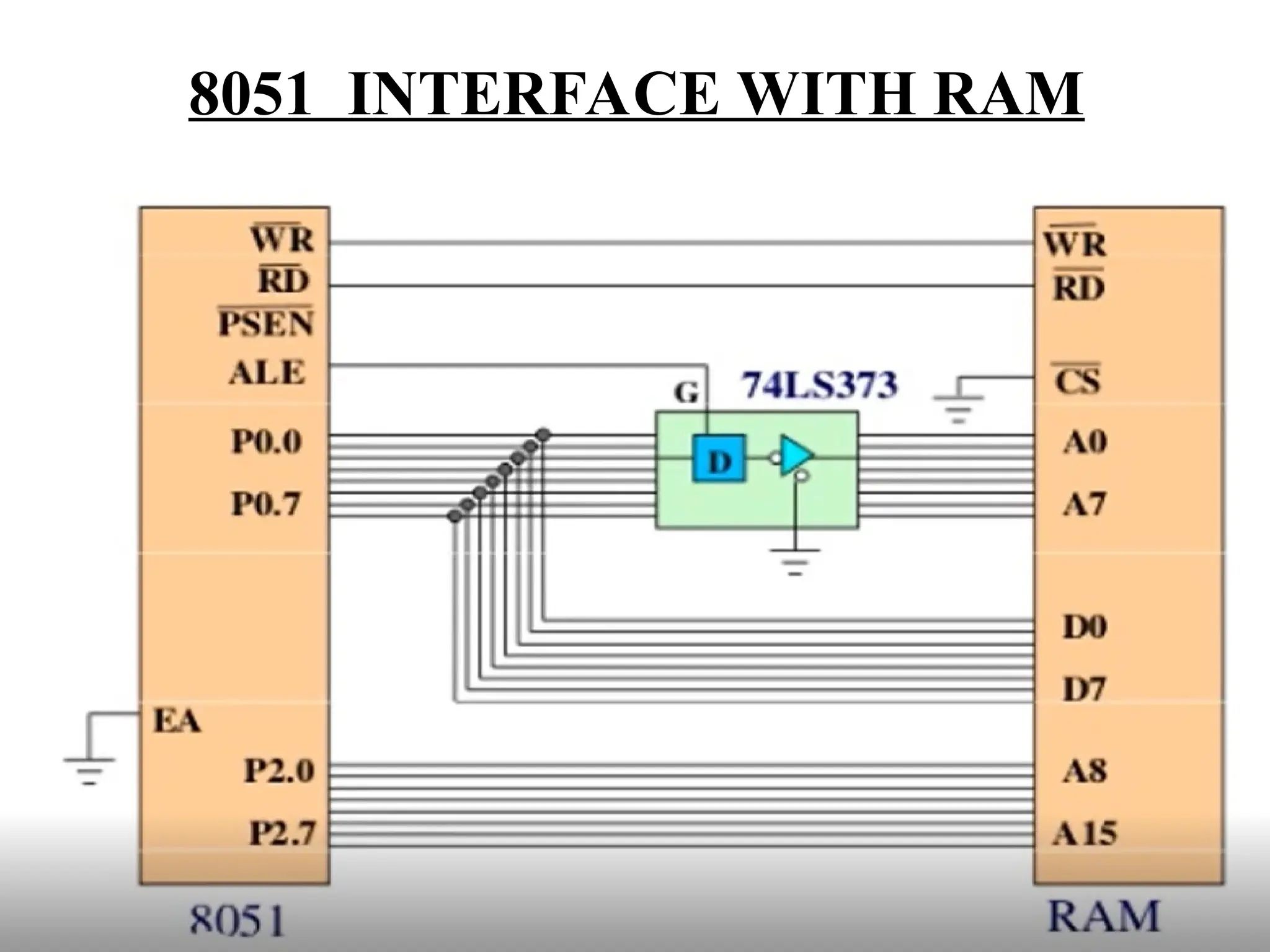
• The 8051is a 40 pin device. Out of these 40 pins, 32 are used for I/O. • 24 of these are dual purpose, i.e. they can operate as I/O or a control line or as part of address or data bus.
21.
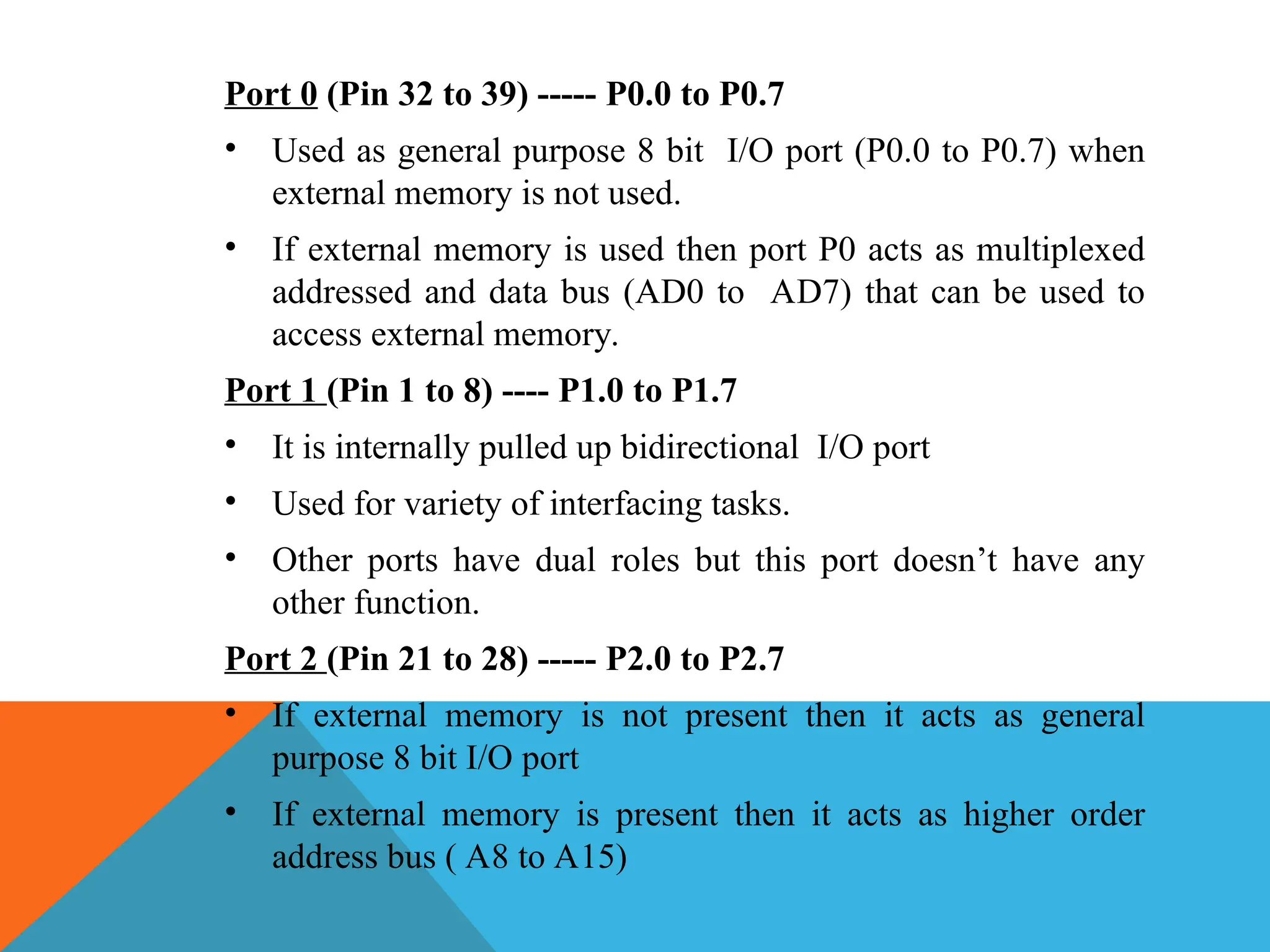
Port 0 (Pin32 to 39) ----- P0.0 to P0.7 • Used as general purpose 8 bit I/O port (P0.0 to P0.7) when external memory is not used. • If external memory is used then port P0 acts as multiplexed addressed and data bus (AD0 to AD7) that can be used to access external memory. Port 1 (Pin 1 to 8) ---- P1.0 to P1.7 • It is internally pulled up bidirectional I/O port • Used for variety of interfacing tasks. • Other ports have dual roles but this port doesn’t have any other function. Port 2 (Pin 21 to 28) ----- P2.0 to P2.7 • If external memory is not present then it acts as general purpose 8 bit I/O port • If external memory is present then it acts as higher order address bus ( A8 to A15)
22.
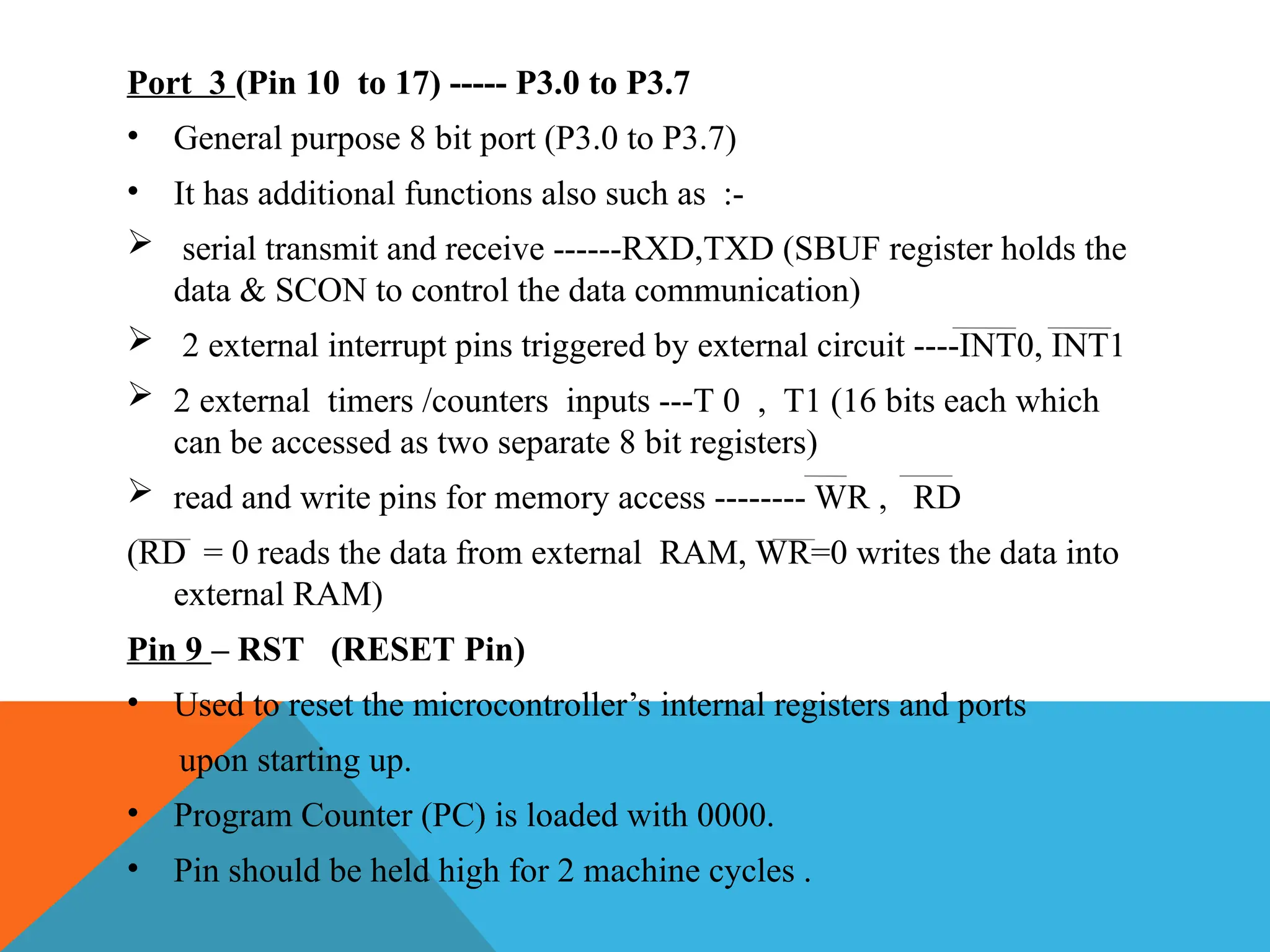
Port 3 (Pin10 to 17) ----- P3.0 to P3.7 • General purpose 8 bit port (P3.0 to P3.7) • It has additional functions also such as :- serial transmit and receive ------RXD,TXD (SBUF register holds the data & SCON to control the data communication) 2 external interrupt pins triggered by external circuit ----INT0, INT1 2 external timers /counters inputs ---T 0 , T1 (16 bits each which can be accessed as two separate 8 bit registers) read and write pins for memory access -------- WR , RD (RD = 0 reads the data from external RAM, WR=0 writes the data into external RAM) Pin 9 – RST (RESET Pin) • Used to reset the microcontroller’s internal registers and ports upon starting up. • Program Counter (PC) is loaded with 0000. • Pin should be held high for 2 machine cycles .
23.
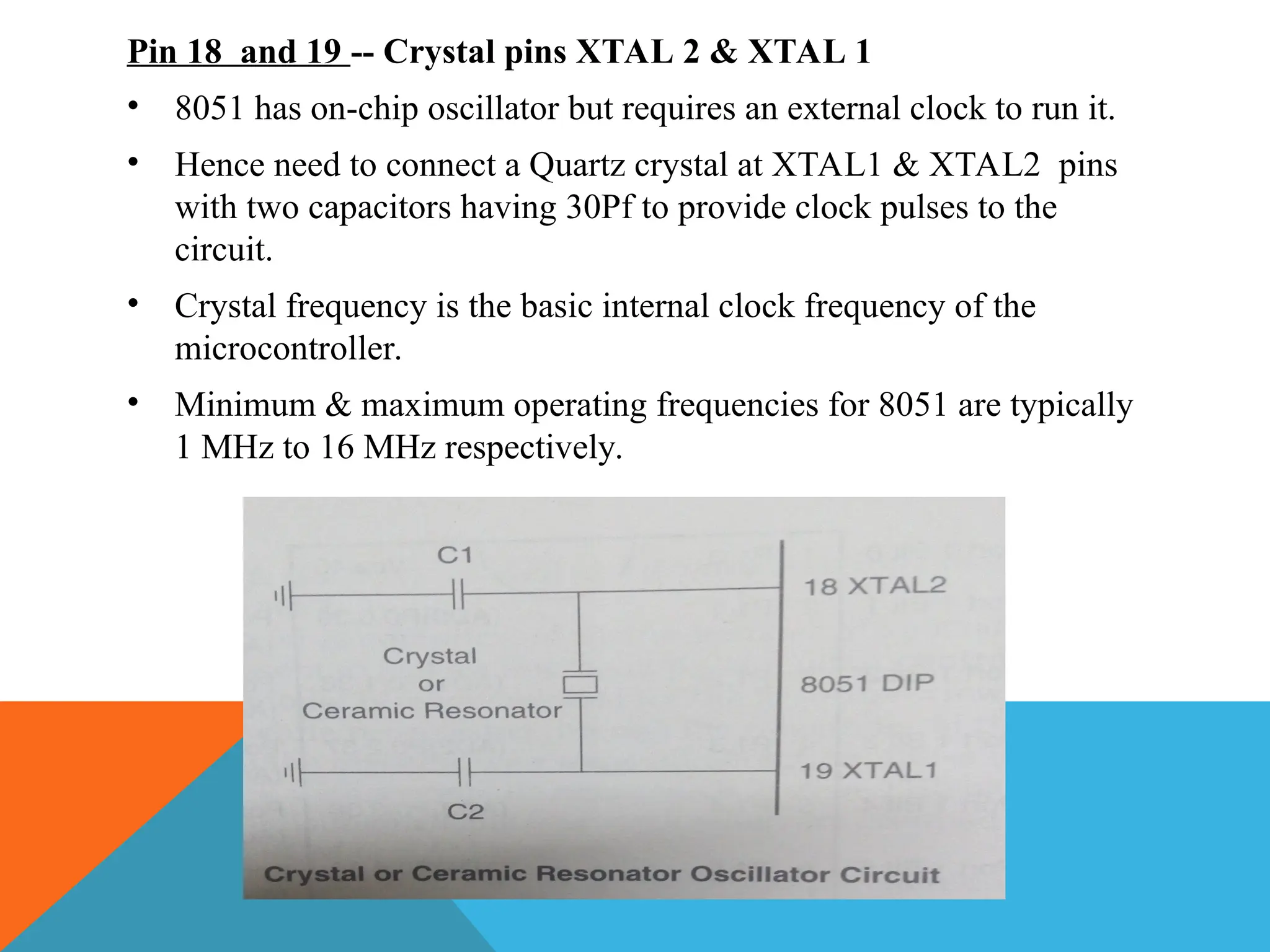
Pin 18 and19 -- Crystal pins XTAL 2 & XTAL 1 • 8051 has on-chip oscillator but requires an external clock to run it. • Hence need to connect a Quartz crystal at XTAL1 & XTAL2 pins with two capacitors having 30Pf to provide clock pulses to the circuit. • Crystal frequency is the basic internal clock frequency of the microcontroller. • Minimum & maximum operating frequencies for 8051 are typically 1 MHz to 16 MHz respectively.
24.
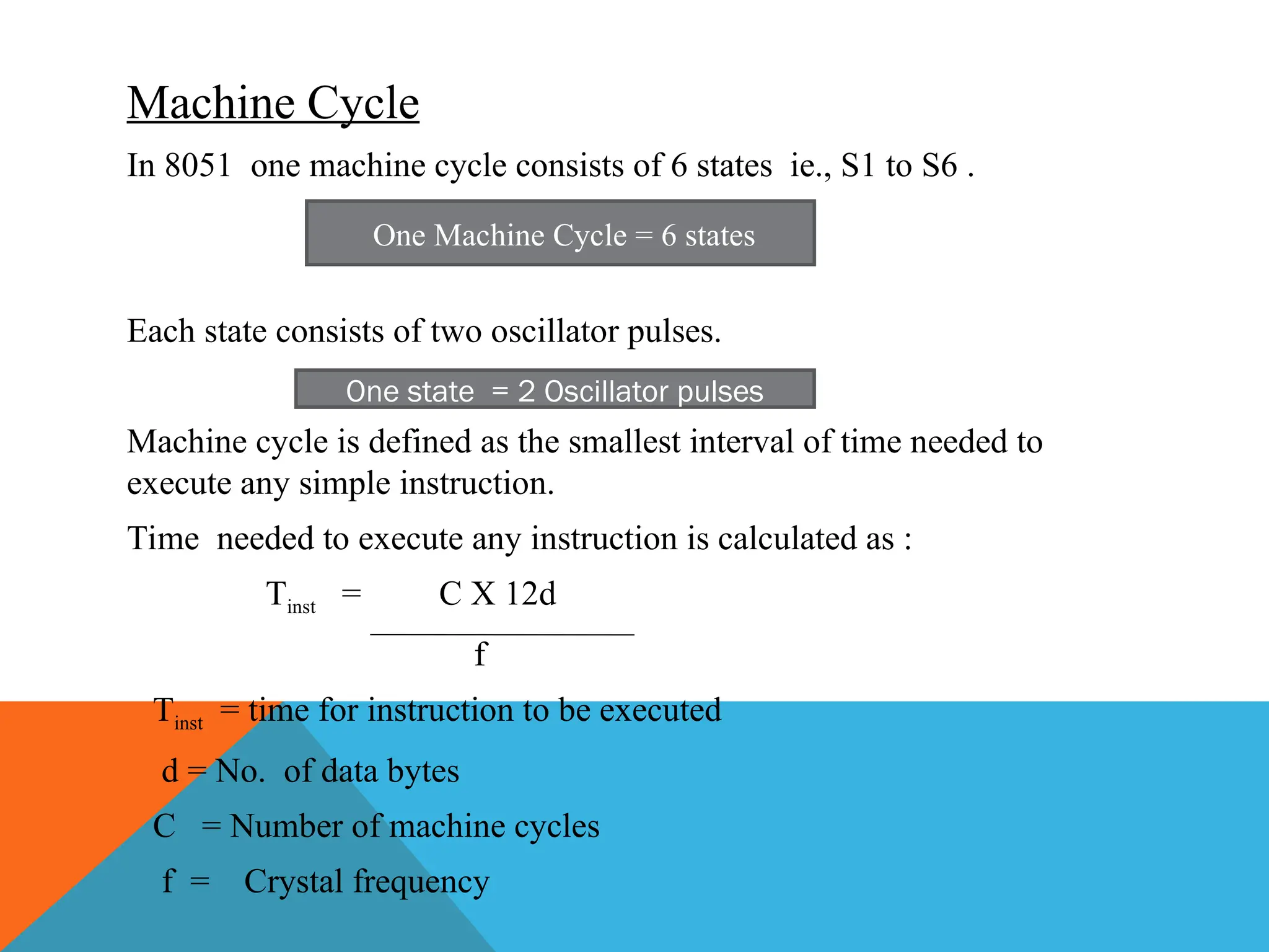
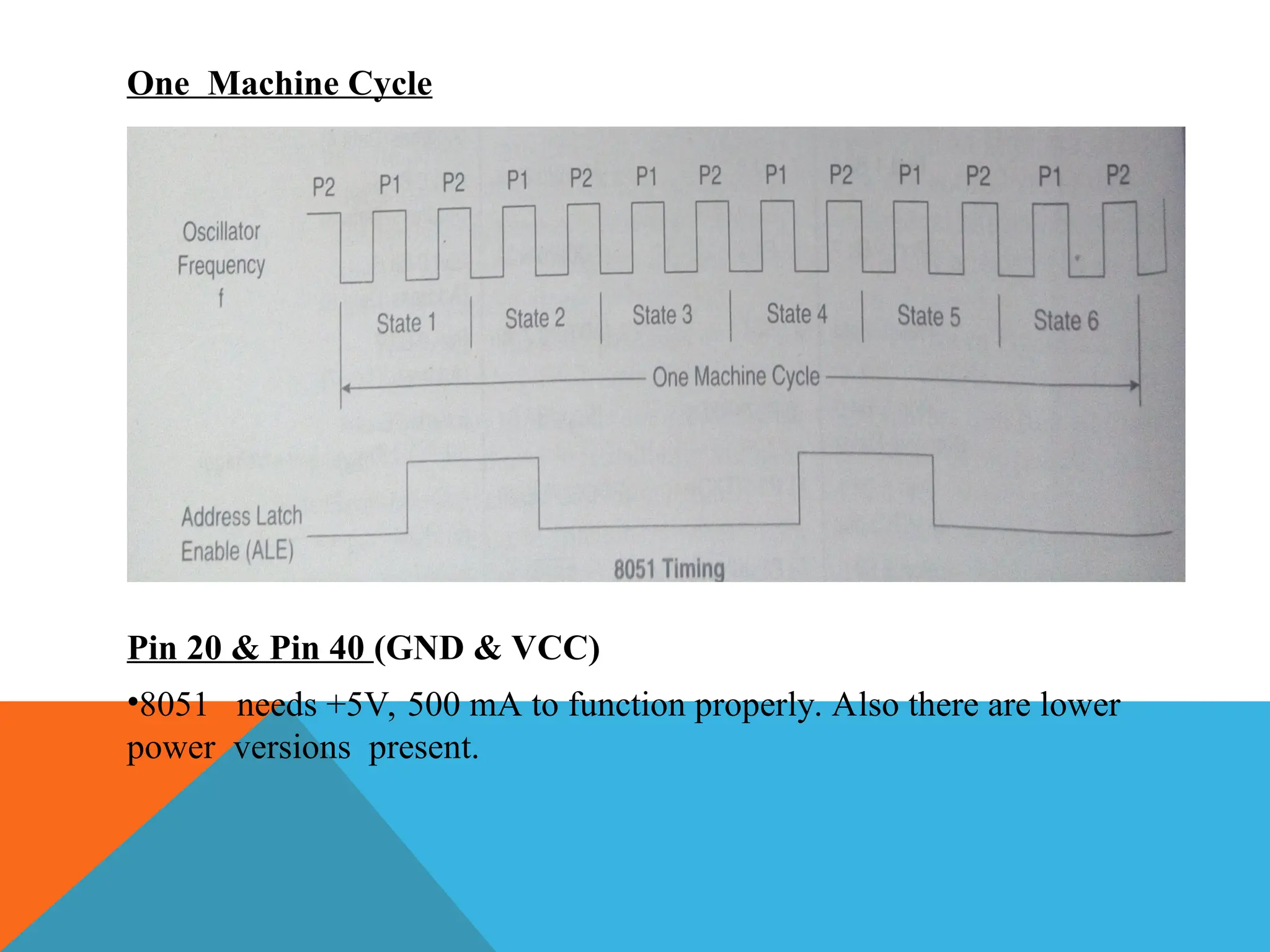
Machine Cycle In 8051one machine cycle consists of 6 states ie., S1 to S6 . Each state consists of two oscillator pulses. Machine cycle is defined as the smallest interval of time needed to execute any simple instruction. Time needed to execute any instruction is calculated as : Tinst = C X 12d f Tinst = time for instruction to be executed d = No. of data bytes C = Number of machine cycles f = Crystal frequency One Machine Cycle = 6 states One state = 2 Oscillator pulses
25.
One Machine Cycle Pin20 & Pin 40 (GND & VCC) •8051 needs +5V, 500 mA to function properly. Also there are lower power versions present.
26.
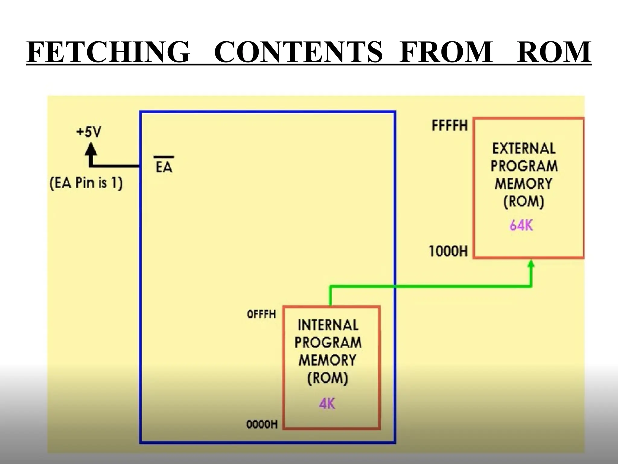
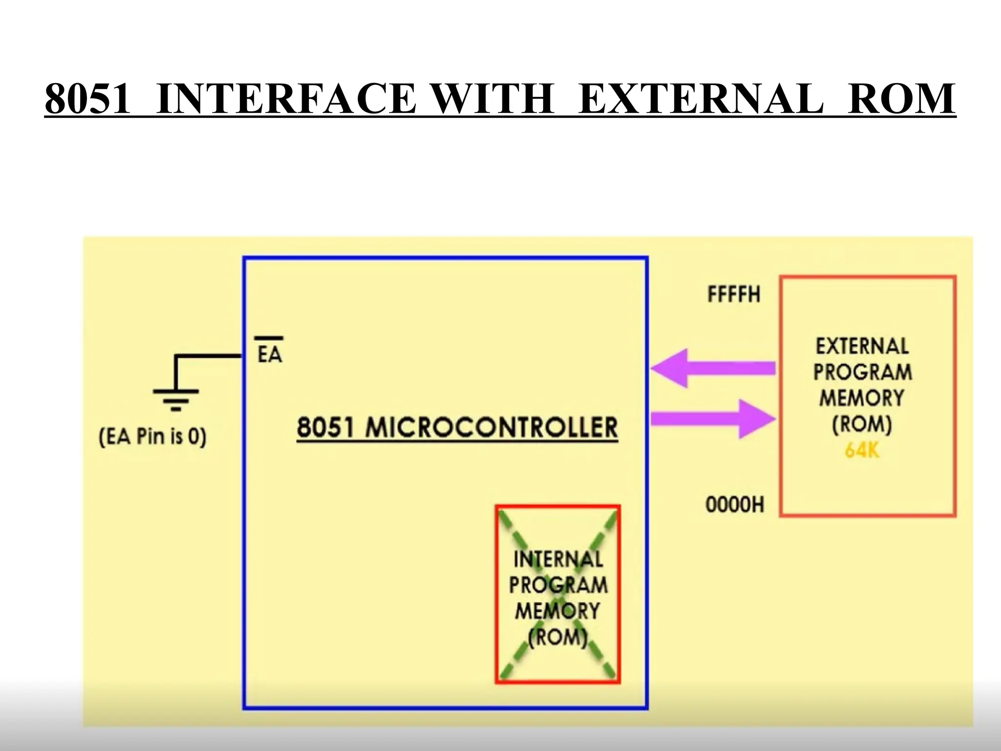
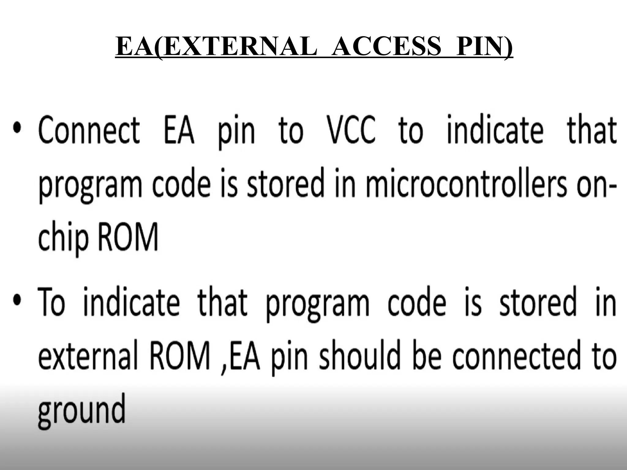
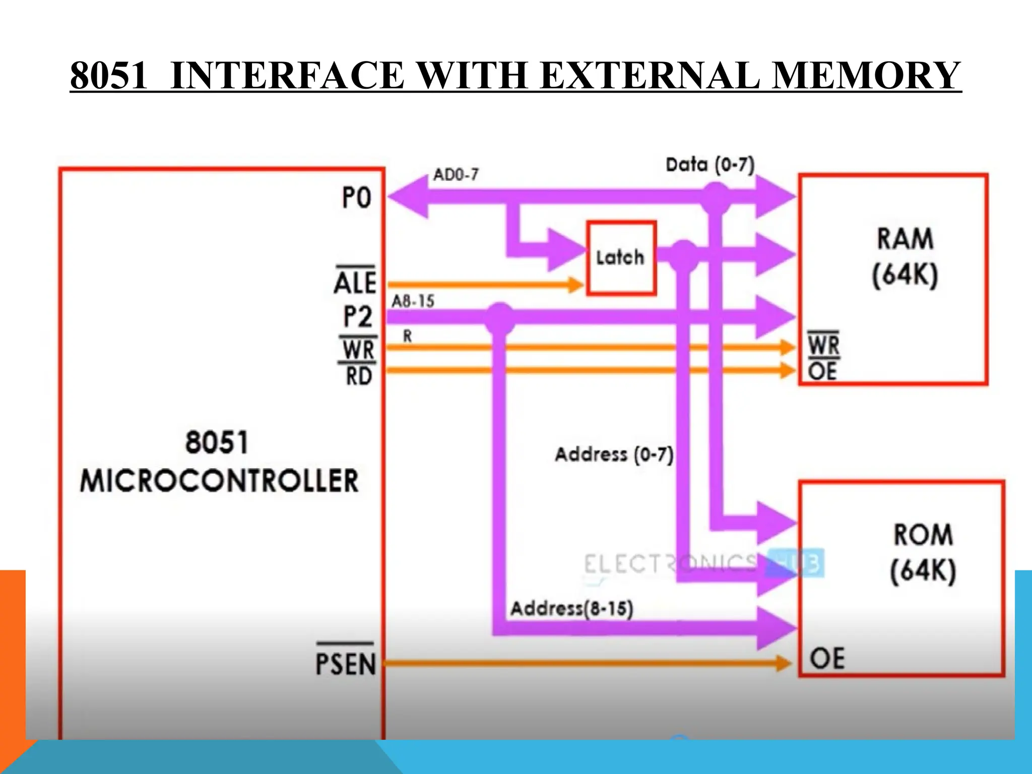
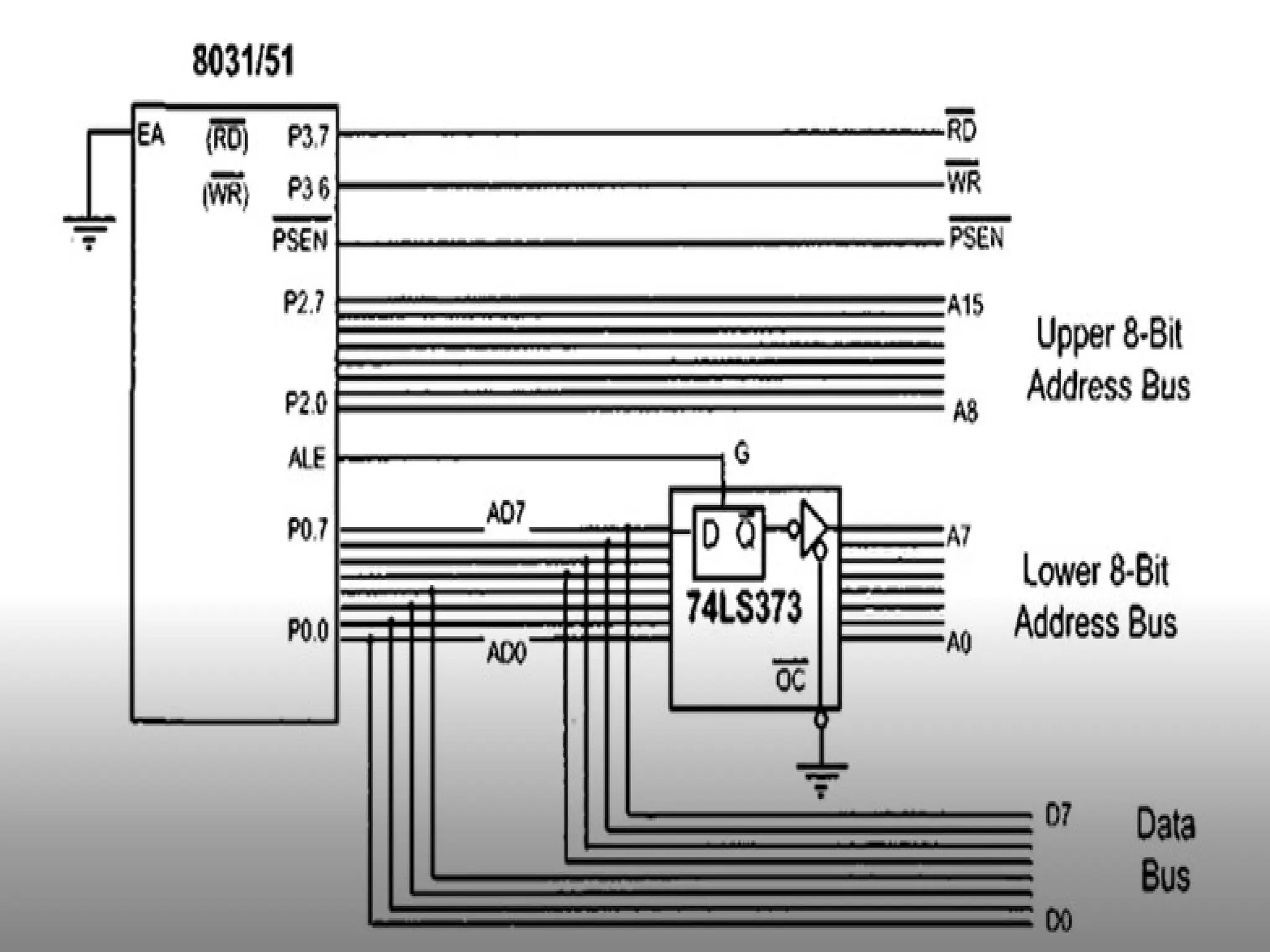
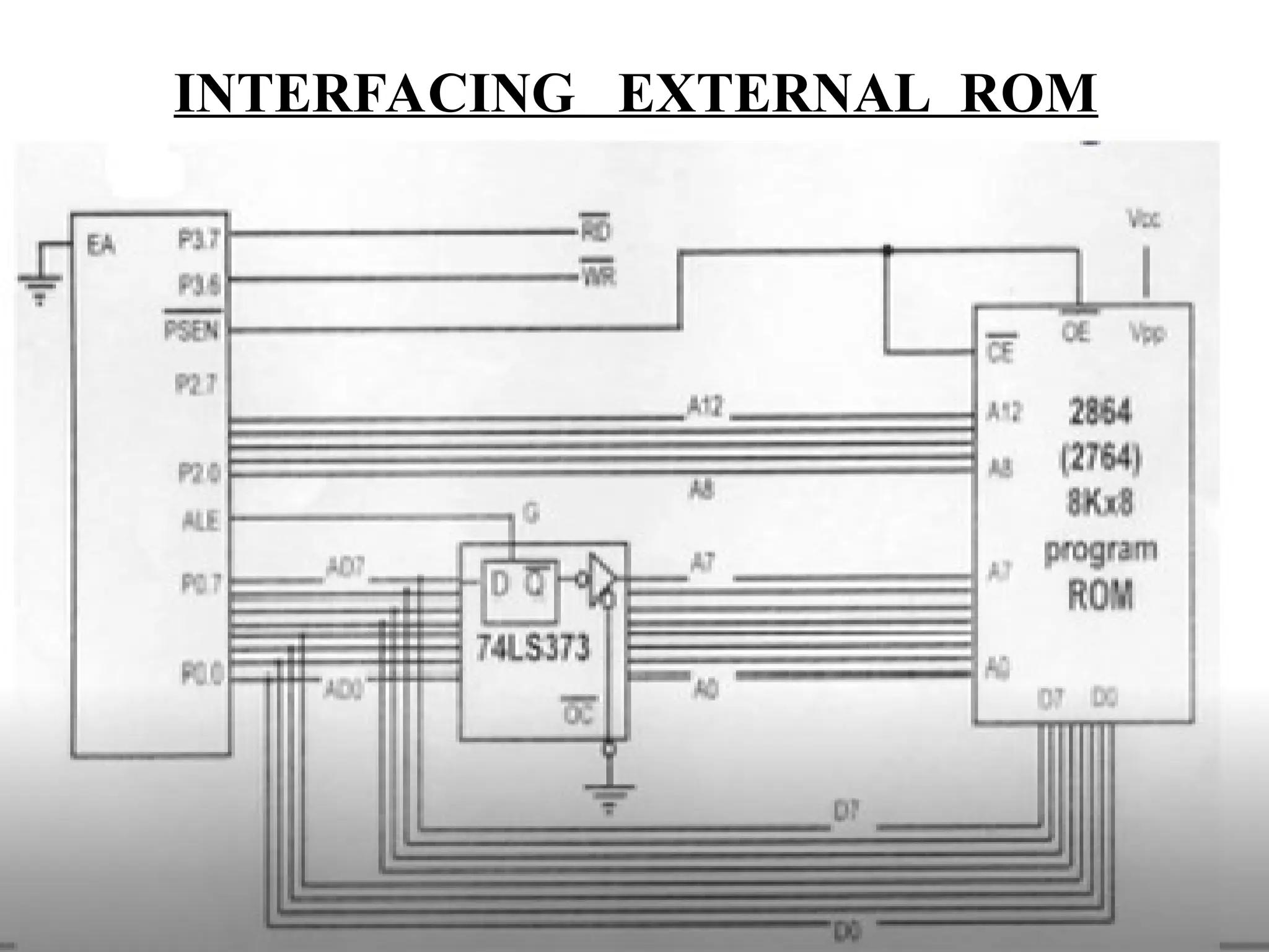
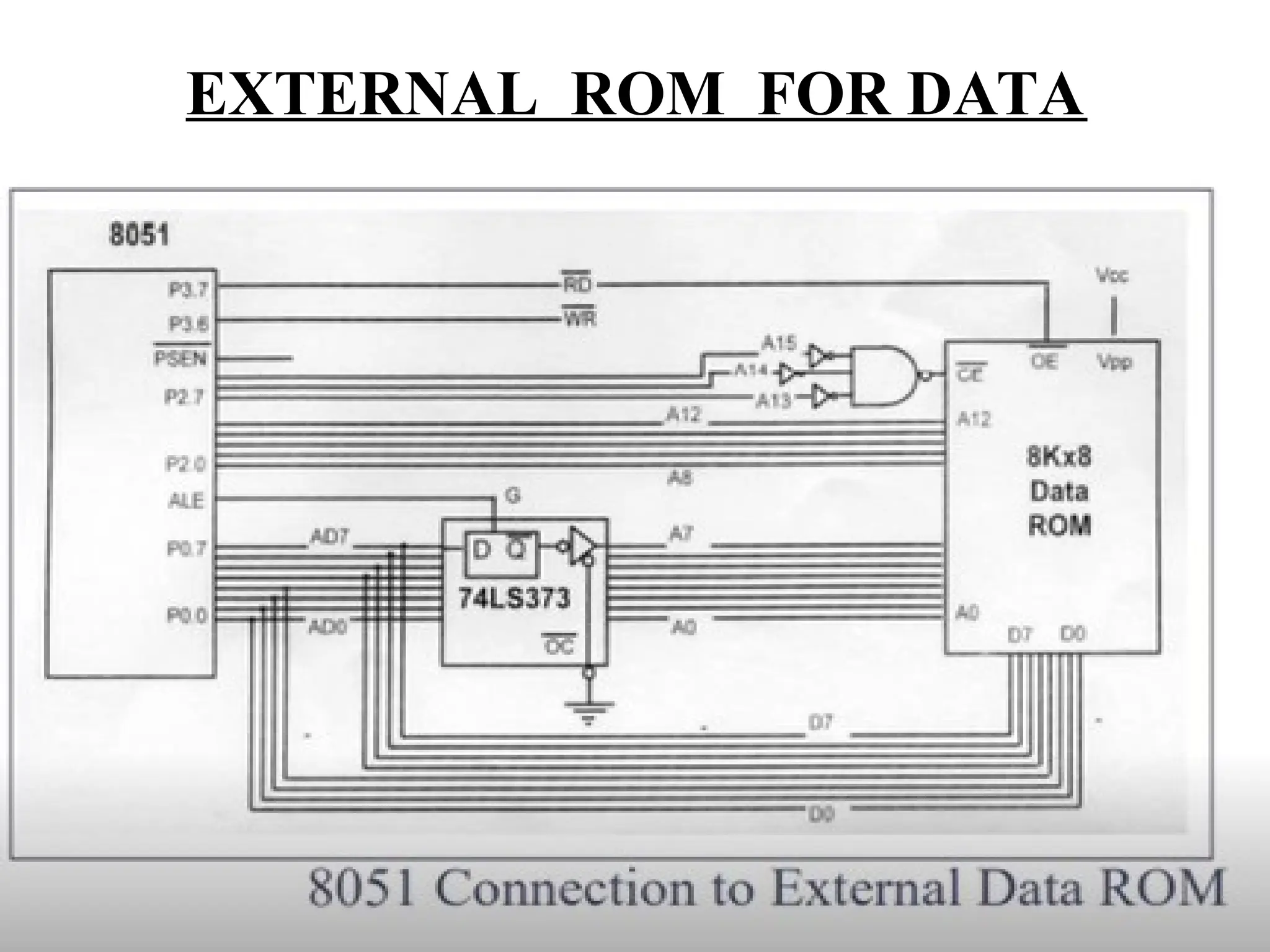
Pin 29----- PSEN( Program Store Enable) • In order to use the external memory it is required to provide the low voltage at both pins PSEN and EA pins. • Used to read signal from external program memory. Pin 30-----ALE (Address Latch Enable) • Used when multiple memory chips are connected to the controller and only one of them needs to be selected. • Used to demultiplex the address and data bus. • When ALE=1 Port 0 is used as lower order address lines(A0 to A7) • When ALE=0 Port 0 is used as data lines. Pin 31 -----EA /VPP (External Access) • Used to enable / disable the external memory interfacing. • EA=0 indicates the presence of external memory. Then code is stored in external ROM. Program is fetched from address location 0000 to FFFFh. • When EA = 1 Code is stored in internal ROM & program is fetched from address location 0000 to 0FFFh.
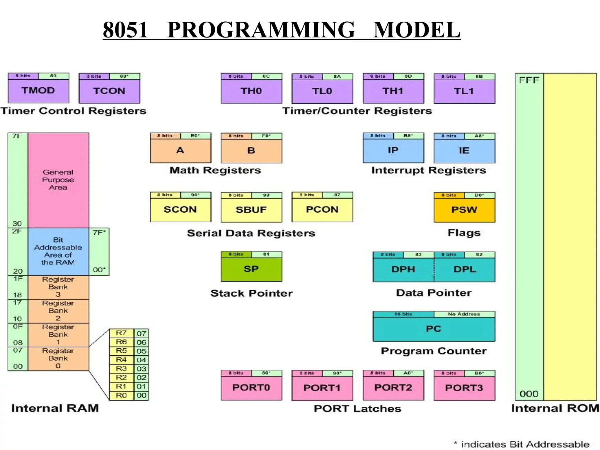
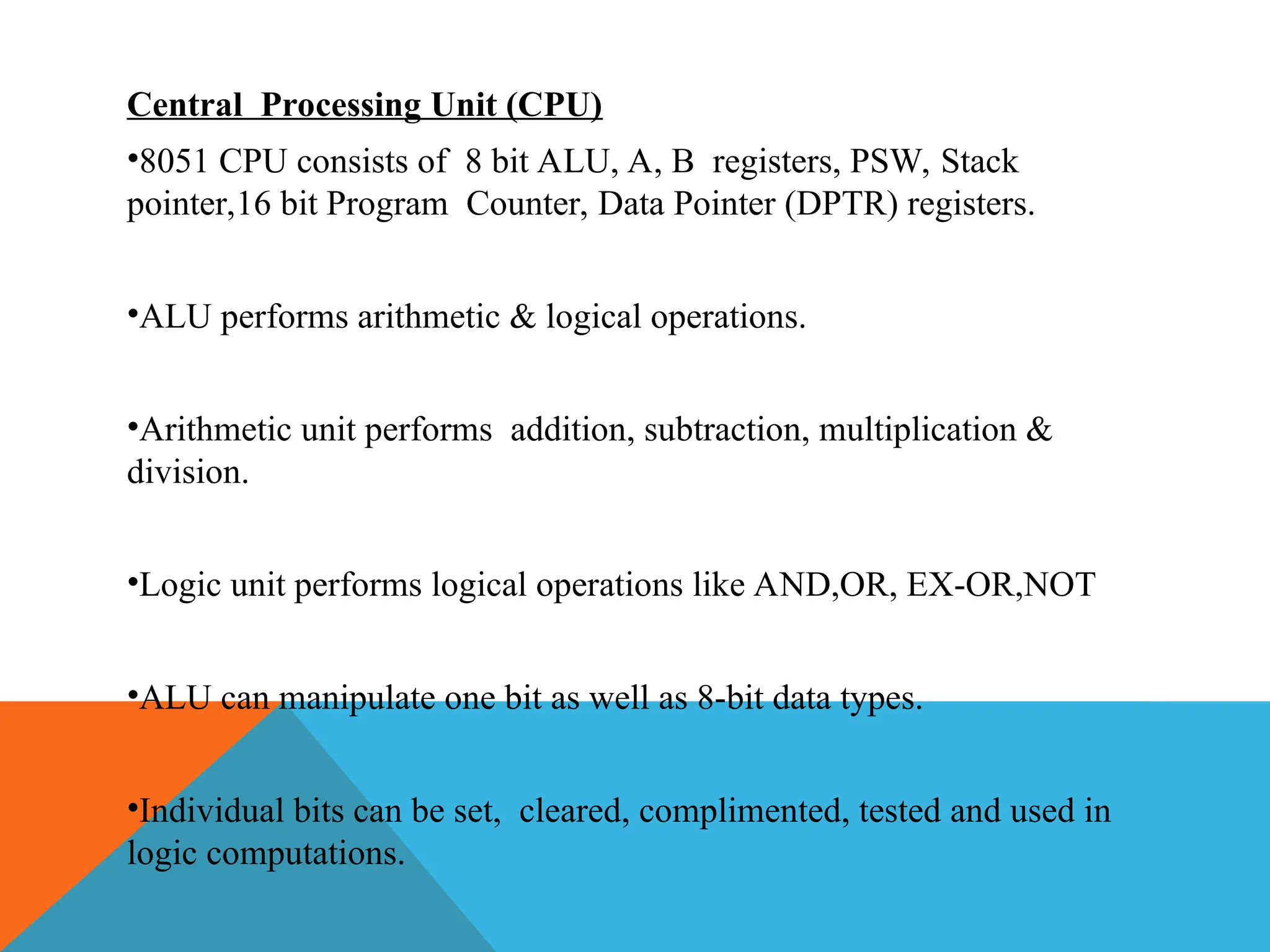
Central Processing Unit(CPU) •8051 CPU consists of 8 bit ALU, A, B registers, PSW, Stack pointer,16 bit Program Counter, Data Pointer (DPTR) registers. •ALU performs arithmetic & logical operations. •Arithmetic unit performs addition, subtraction, multiplication & division. •Logic unit performs logical operations like AND,OR, EX-OR,NOT •ALU can manipulate one bit as well as 8-bit data types. •Individual bits can be set, cleared, complimented, tested and used in logic computations.
30.
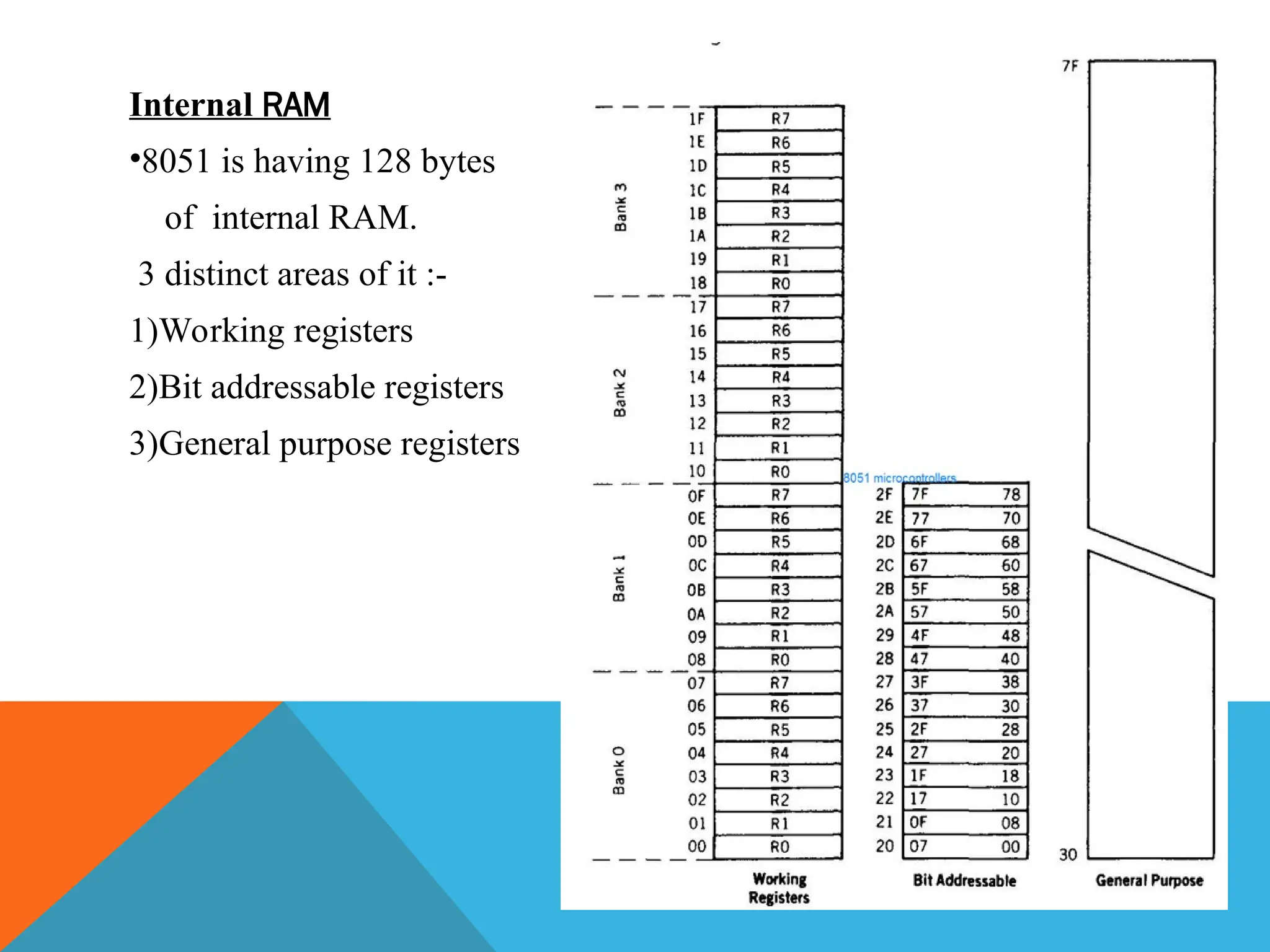
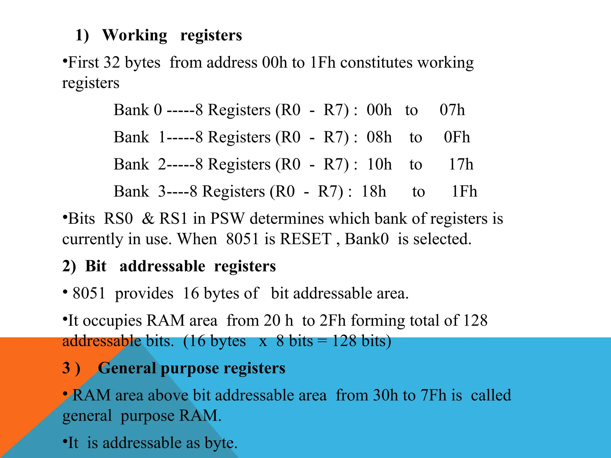
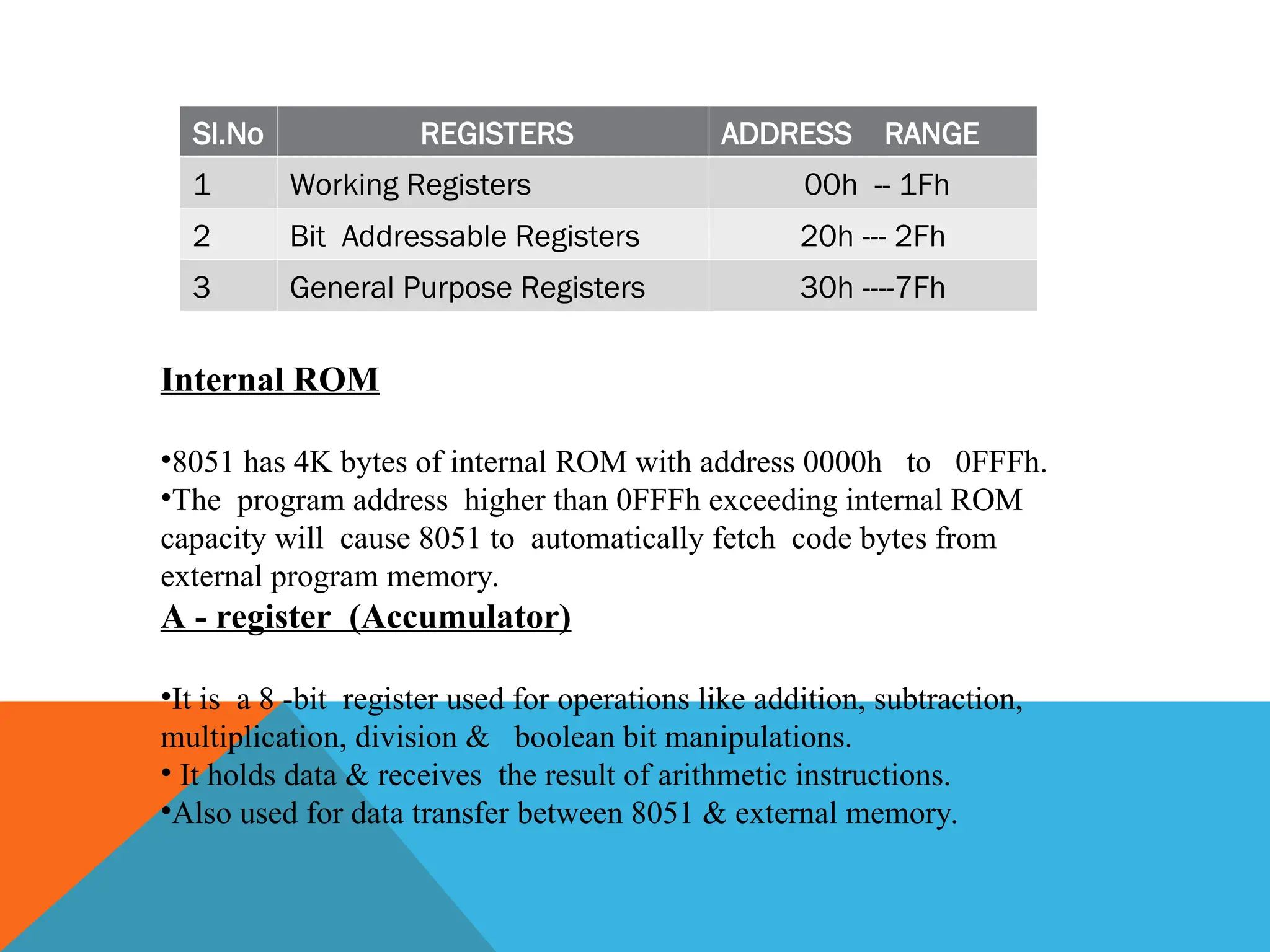
Internal RAM •8051 ishaving 128 bytes of internal RAM. 3 distinct areas of it :- 1)Working registers 2)Bit addressable registers 3)General purpose registers
31.
1) Working registers •First32 bytes from address 00h to 1Fh constitutes working registers Bank 0 -----8 Registers (R0 - R7) : 00h to 07h Bank 1-----8 Registers (R0 - R7) : 08h to 0Fh Bank 2-----8 Registers (R0 - R7) : 10h to 17h Bank 3----8 Registers (R0 - R7) : 18h to 1Fh •Bits RS0 & RS1 in PSW determines which bank of registers is currently in use. When 8051 is RESET , Bank0 is selected. 2) Bit addressable registers • 8051 provides 16 bytes of bit addressable area. •It occupies RAM area from 20 h to 2Fh forming total of 128 addressable bits. (16 bytes x 8 bits = 128 bits) 3 ) General purpose registers • RAM area above bit addressable area from 30h to 7Fh is called general purpose RAM. •It is addressable as byte.
32.
Sl.No REGISTERS ADDRESSRANGE 1 Working Registers 00h -- 1Fh 2 Bit Addressable Registers 20h --- 2Fh 3 General Purpose Registers 30h ----7Fh Internal ROM •8051 has 4K bytes of internal ROM with address 0000h to 0FFFh. •The program address higher than 0FFFh exceeding internal ROM capacity will cause 8051 to automatically fetch code bytes from external program memory. A - register (Accumulator) •It is a 8 -bit register used for operations like addition, subtraction, multiplication, division & boolean bit manipulations. • It holds data & receives the result of arithmetic instructions. •Also used for data transfer between 8051 & external memory.
33.
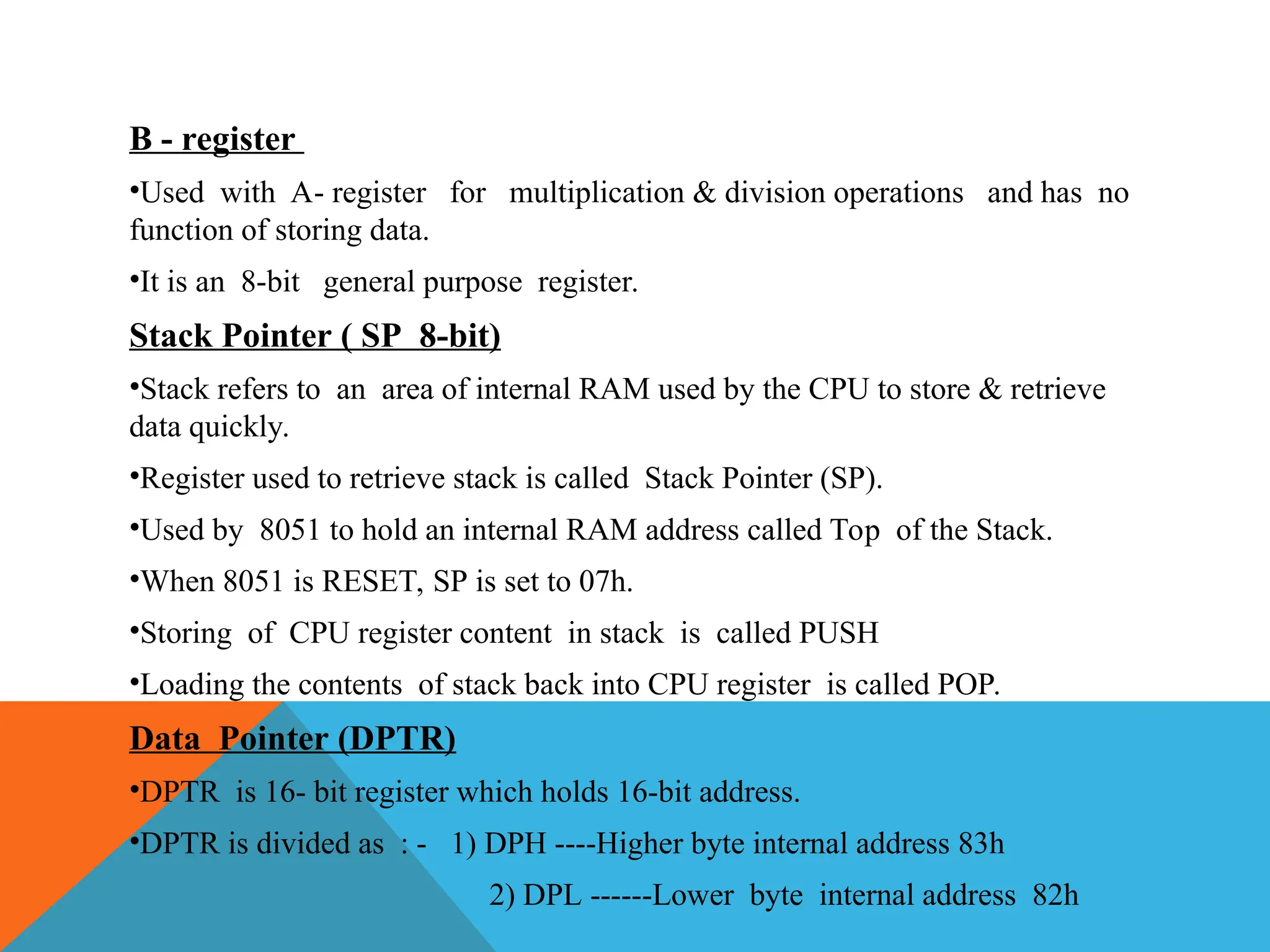
B - register •Usedwith A- register for multiplication & division operations and has no function of storing data. •It is an 8-bit general purpose register. Stack Pointer ( SP 8-bit) •Stack refers to an area of internal RAM used by the CPU to store & retrieve data quickly. •Register used to retrieve stack is called Stack Pointer (SP). •Used by 8051 to hold an internal RAM address called Top of the Stack. •When 8051 is RESET, SP is set to 07h. •Storing of CPU register content in stack is called PUSH •Loading the contents of stack back into CPU register is called POP. Data Pointer (DPTR) •DPTR is 16- bit register which holds 16-bit address. •DPTR is divided as : - 1) DPH ----Higher byte internal address 83h 2) DPL ------Lower byte internal address 82h
34.
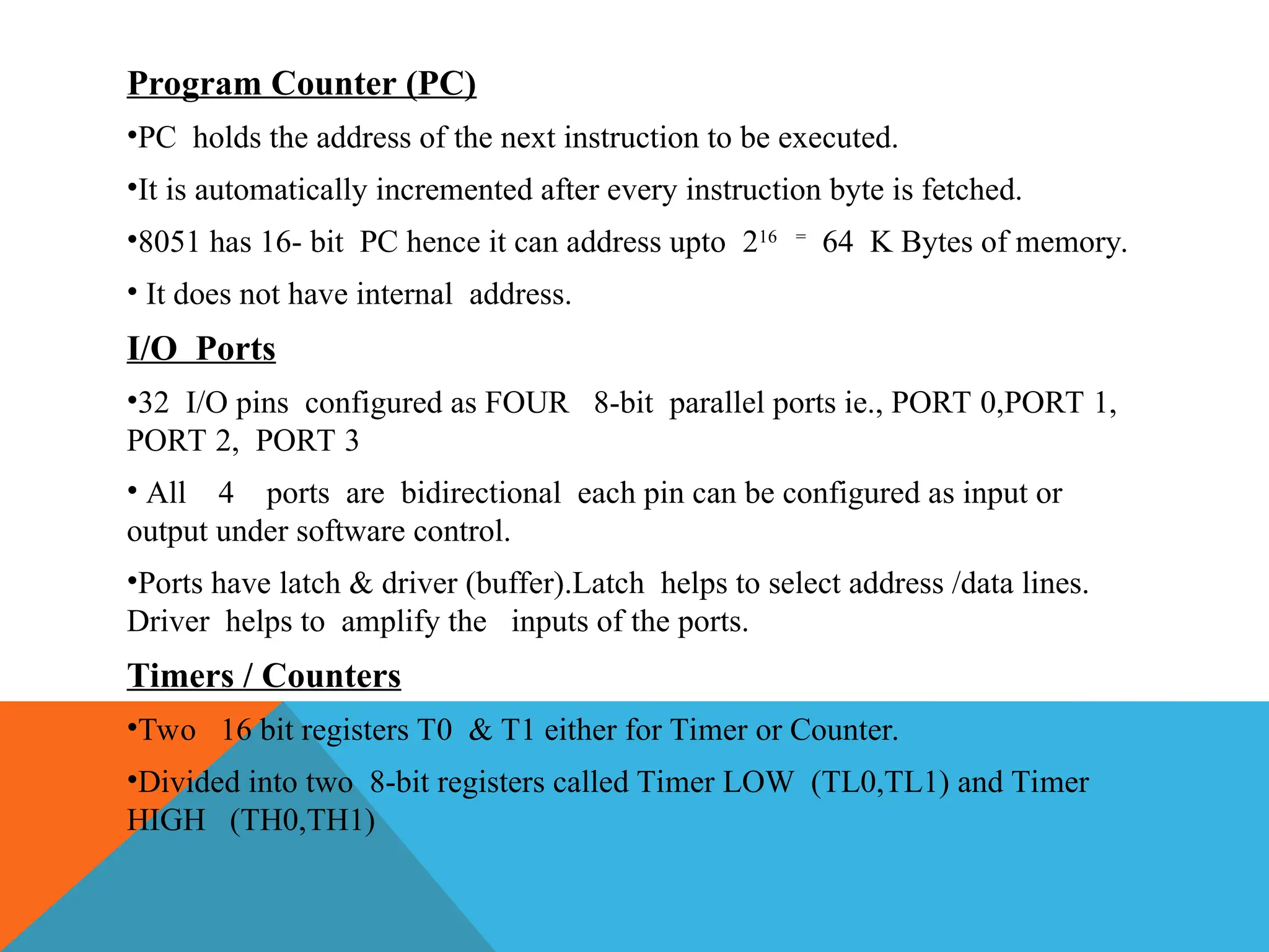
Program Counter (PC) •PCholds the address of the next instruction to be executed. •It is automatically incremented after every instruction byte is fetched. •8051 has 16- bit PC hence it can address upto 216 = 64 K Bytes of memory. • It does not have internal address. I/O Ports •32 I/O pins configured as FOUR 8-bit parallel ports ie., PORT 0,PORT 1, PORT 2, PORT 3 • All 4 ports are bidirectional each pin can be configured as input or output under software control. •Ports have latch & driver (buffer).Latch helps to select address /data lines. Driver helps to amplify the inputs of the ports. Timers / Counters •Two 16 bit registers T0 & T1 either for Timer or Counter. •Divided into two 8-bit registers called Timer LOW (TL0,TL1) and Timer HIGH (TH0,TH1)
35.
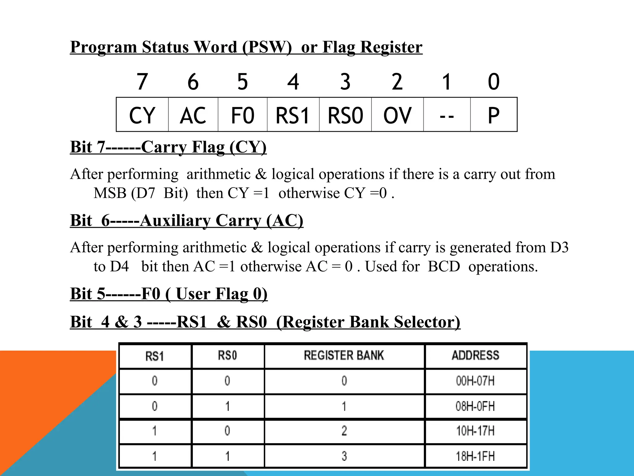
Program Status Word(PSW) or Flag Register Bit 7------Carry Flag (CY) After performing arithmetic & logical operations if there is a carry out from MSB (D7 Bit) then CY =1 otherwise CY =0 . Bit 6-----Auxiliary Carry (AC) After performing arithmetic & logical operations if carry is generated from D3 to D4 bit then AC =1 otherwise AC = 0 . Used for BCD operations. Bit 5------F0 ( User Flag 0) Bit 4 & 3 -----RS1 & RS0 (Register Bank Selector) 7 6 5 4 3 2 1 0 CY AC F0 RS1 RS0 OV -- P
36.
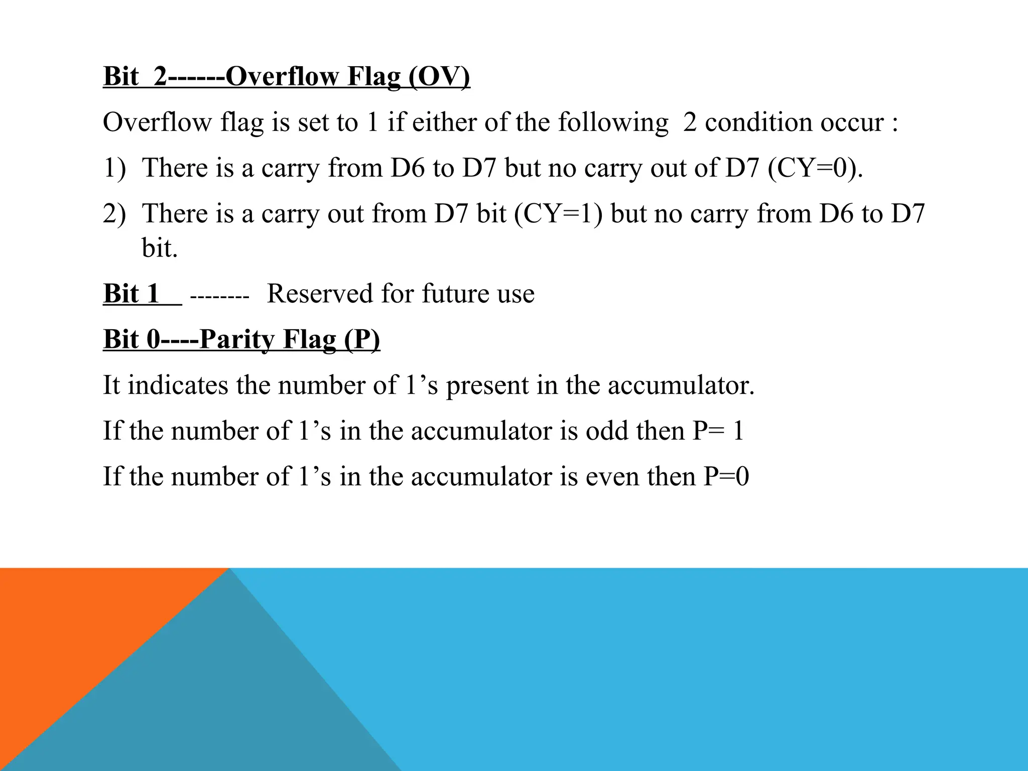
Bit 2------Overflow Flag(OV) Overflow flag is set to 1 if either of the following 2 condition occur : 1) There is a carry from D6 to D7 but no carry out of D7 (CY=0). 2) There is a carry out from D7 bit (CY=1) but no carry from D6 to D7 bit. Bit 1 -------- Reserved for future use Bit 0----Parity Flag (P) It indicates the number of 1’s present in the accumulator. If the number of 1’s in the accumulator is odd then P= 1 If the number of 1’s in the accumulator is even then P=0
37.
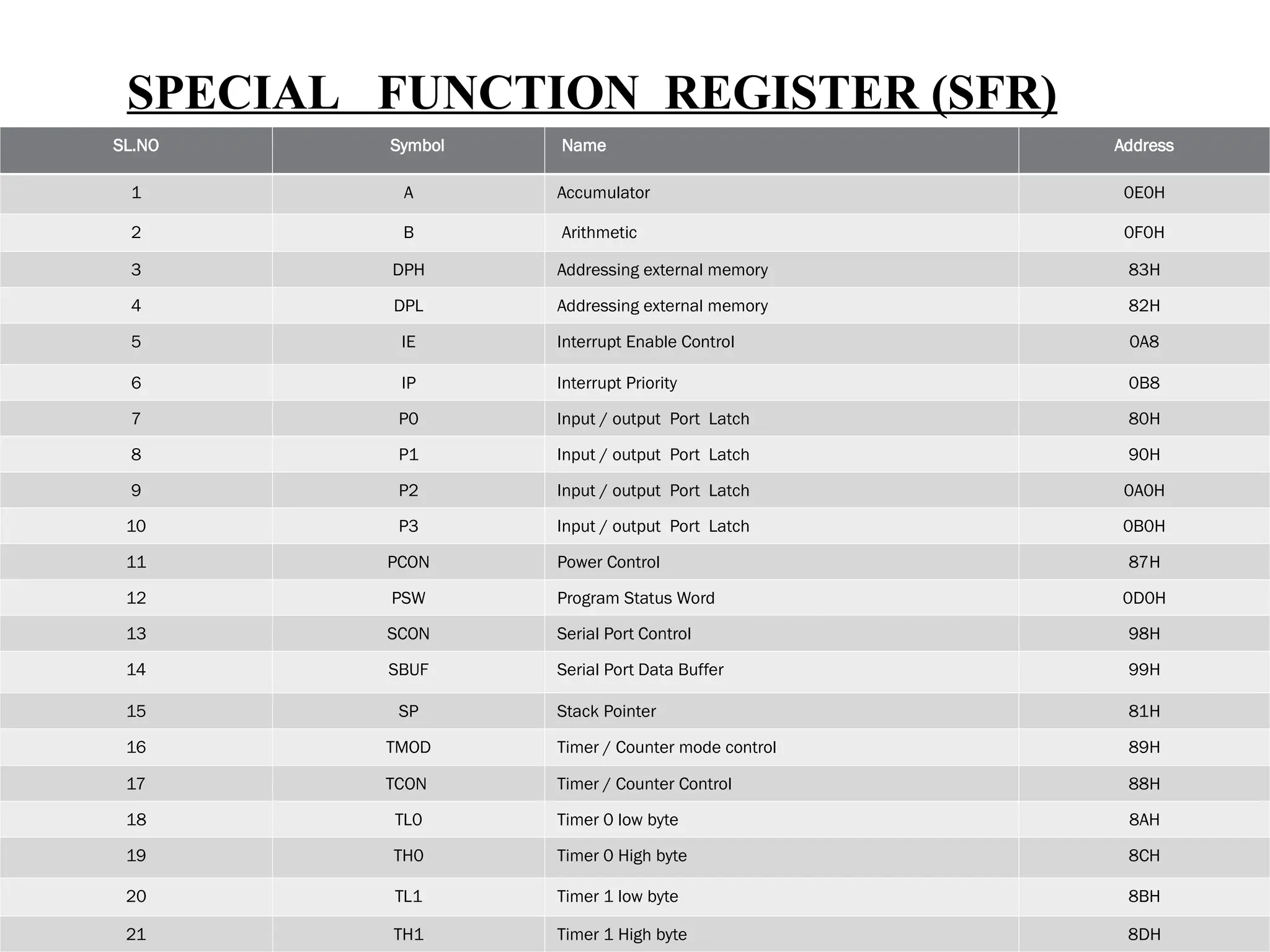
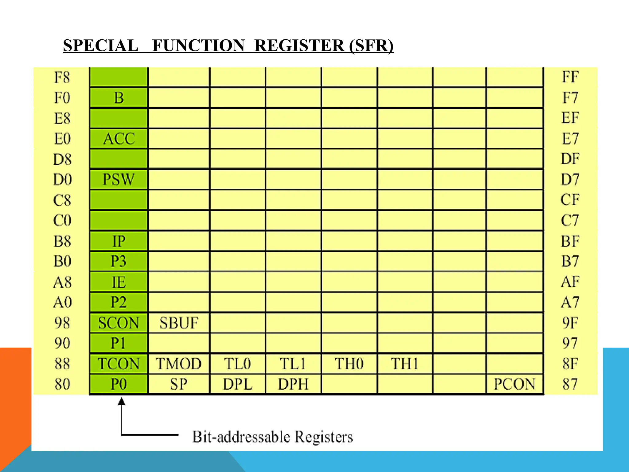
SPECIAL FUNCTION REGISTER(SFR) SL.NO Symbol Name Address 1 A Accumulator 0E0H 2 B Arithmetic 0F0H 3 DPH Addressing external memory 83H 4 DPL Addressing external memory 82H 5 IE Interrupt Enable Control 0A8 6 IP Interrupt Priority 0B8 7 P0 Input / output Port Latch 80H 8 P1 Input / output Port Latch 90H 9 P2 Input / output Port Latch 0A0H 10 P3 Input / output Port Latch 0B0H 11 PCON Power Control 87H 12 PSW Program Status Word 0D0H 13 SCON Serial Port Control 98H 14 SBUF Serial Port Data Buffer 99H 15 SP Stack Pointer 81H 16 TMOD Timer / Counter mode control 89H 17 TCON Timer / Counter Control 88H 18 TL0 Timer 0 low byte 8AH 19 TH0 Timer 0 High byte 8CH 20 TL1 Timer 1 low byte 8BH 21 TH1 Timer 1 High byte 8DH
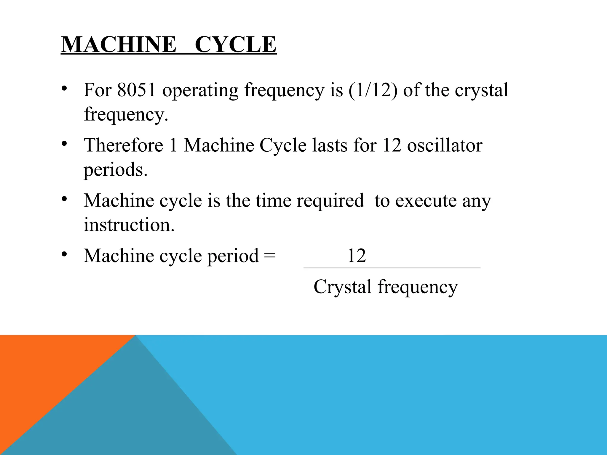
MACHINE CYCLE • For8051 operating frequency is (1/12) of the crystal frequency. • Therefore 1 Machine Cycle lasts for 12 oscillator periods. • Machine cycle is the time required to execute any instruction. • Machine cycle period = 12 Crystal frequency
40.
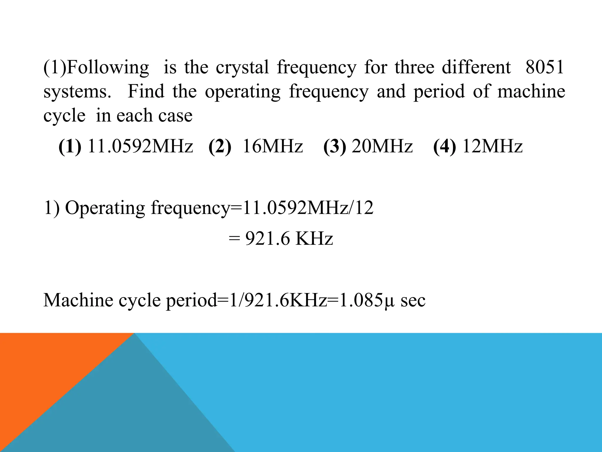
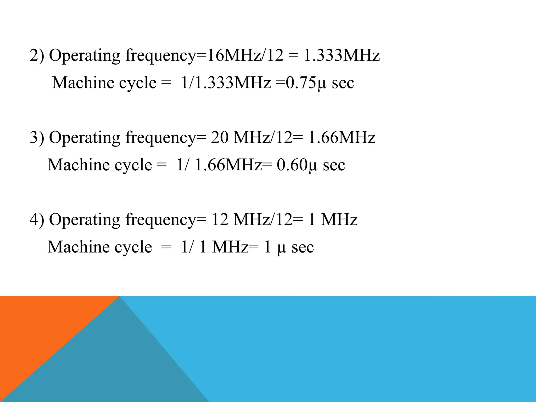
(1)Following is thecrystal frequency for three different 8051 systems. Find the operating frequency and period of machine cycle in each case (1) 11.0592MHz (2) 16MHz (3) 20MHz (4) 12MHz 1) Operating frequency=11.0592MHz/12 = 921.6 KHz Machine cycle period=1/921.6KHz=1.085µ sec
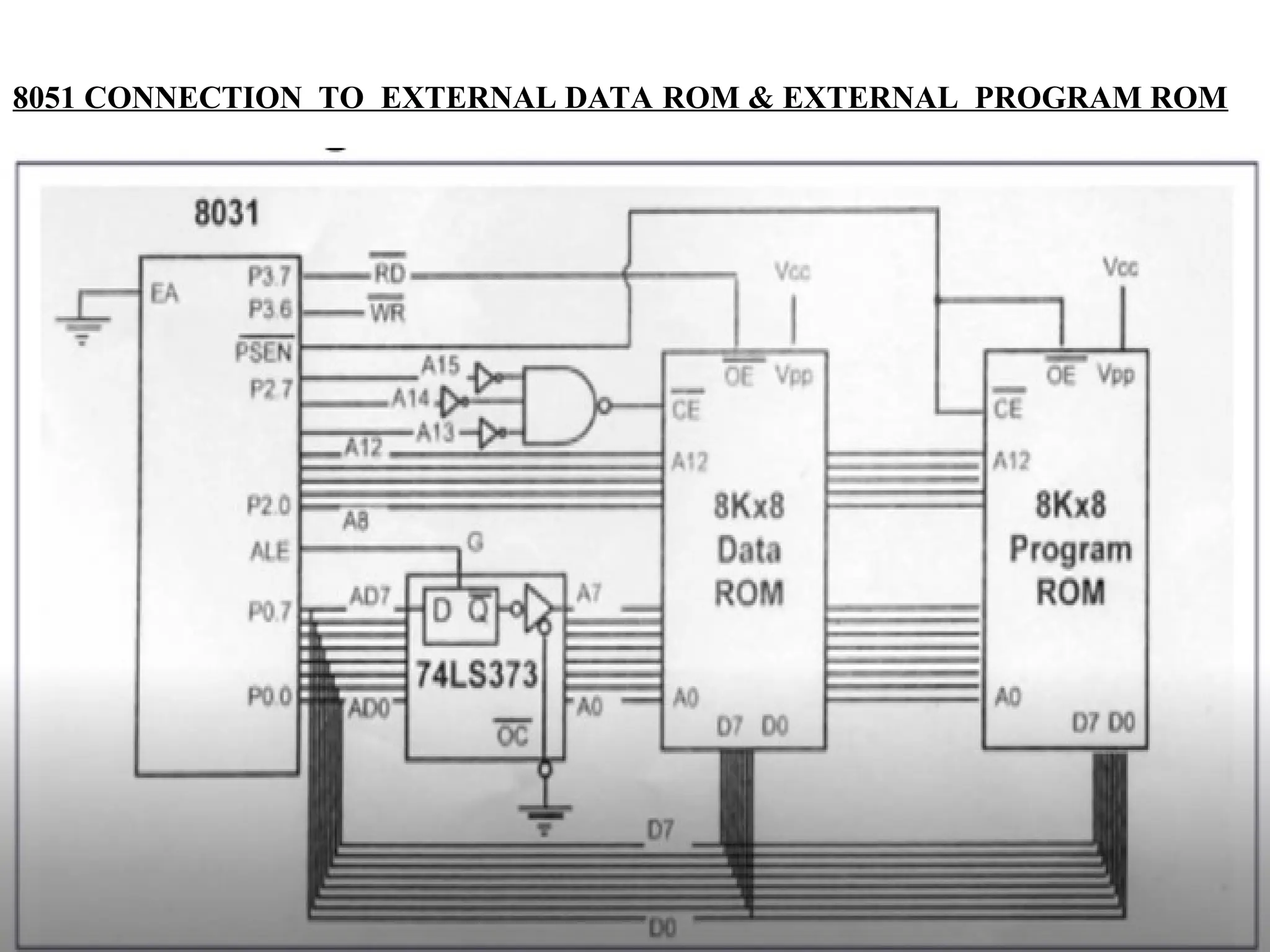
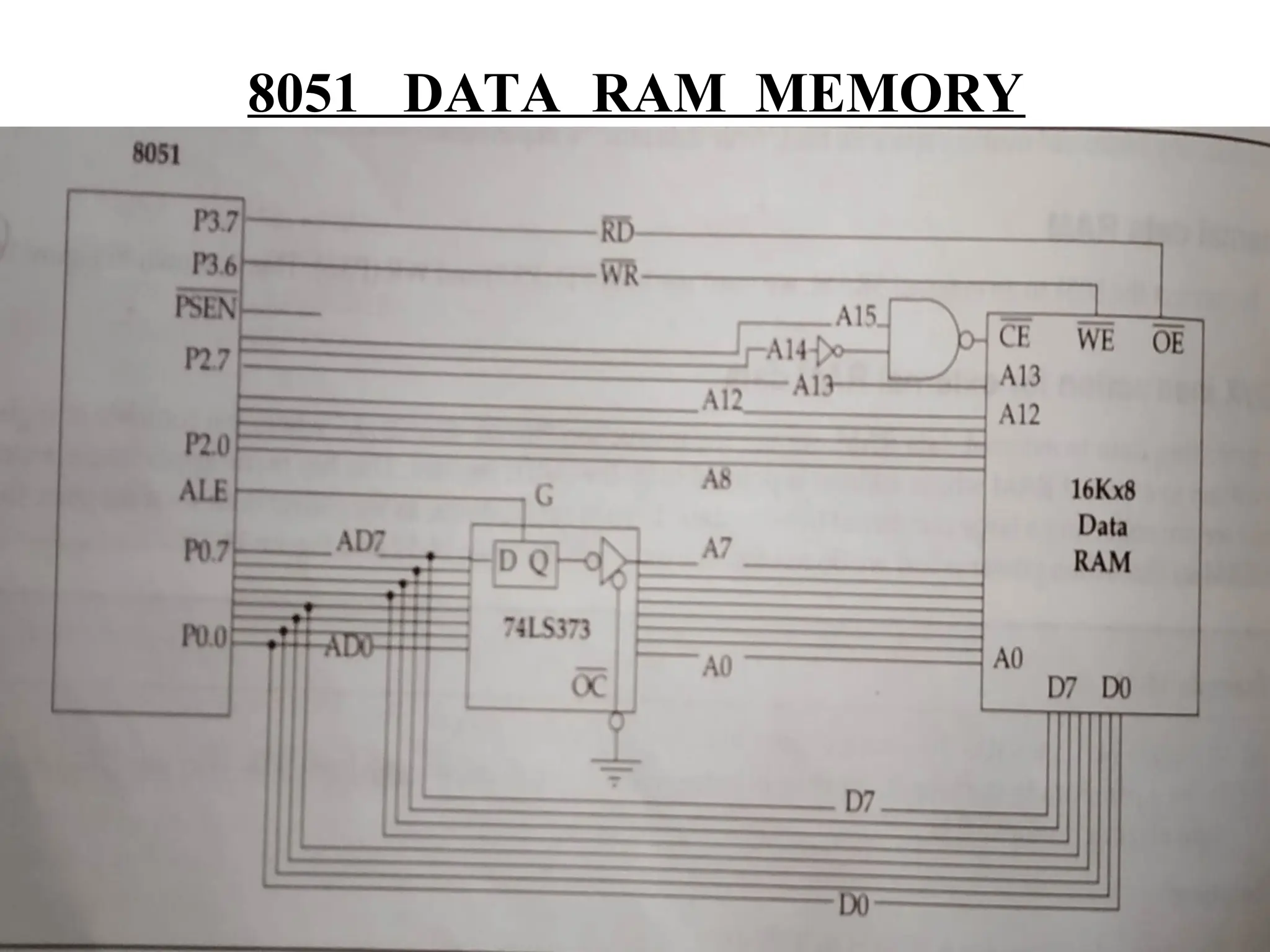
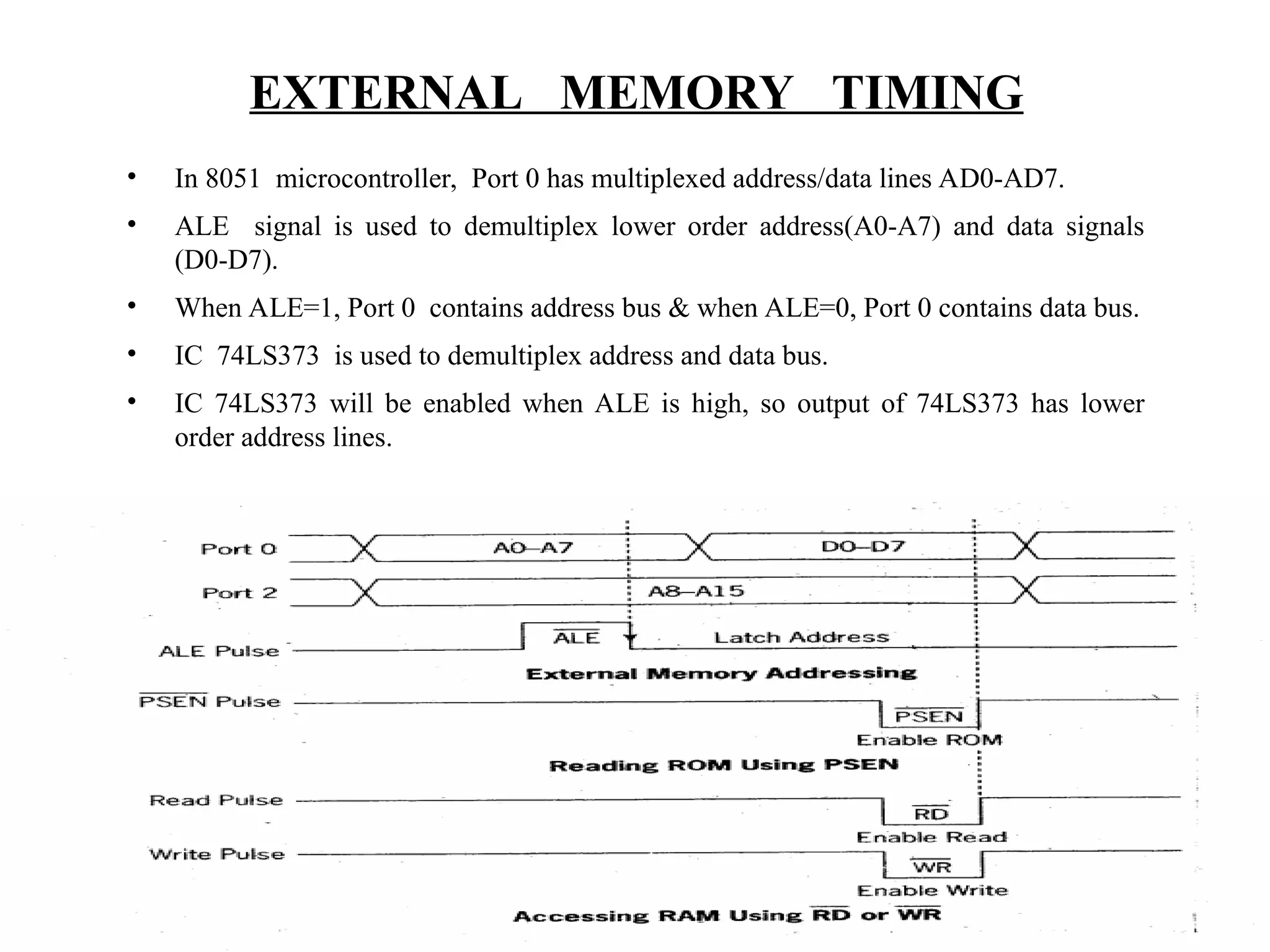
EXTERNAL MEMORY TIMING •In 8051 microcontroller, Port 0 has multiplexed address/data lines AD0-AD7. • ALE signal is used to demultiplex lower order address(A0-A7) and data signals (D0-D7). • When ALE=1, Port 0 contains address bus & when ALE=0, Port 0 contains data bus. • IC 74LS373 is used to demultiplex address and data bus. • IC 74LS373 will be enabled when ALE is high, so output of 74LS373 has lower order address lines.
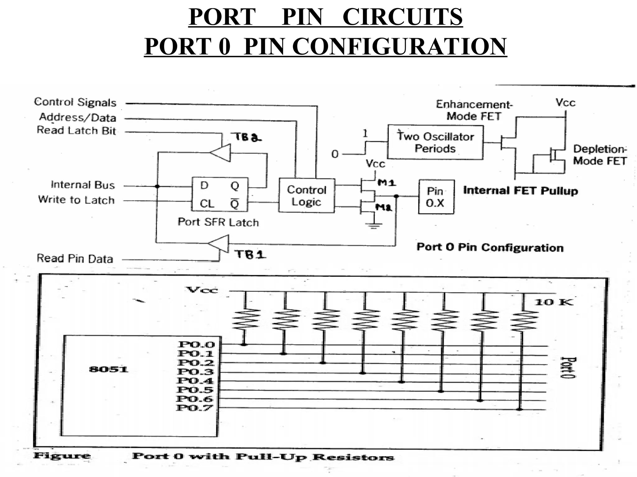
• Port –0 is an 8-bit , bit addressable I/O port. It is also used as a bi-directional low order address and data bus for external memory. • Input Port: To use each pin as an input pin , we must write ‘1’ (LOGIC HIGH) to that bit i.e., 1) Writing ‘1’ to Port-0 pin , the D flip flop output is high i.e., Q=1 & Q=0. 2) Since Q = 0 & is connected to the FET’s gate M1 & M2 ,thus turning OFF both the FET’s. 3) When M1 & M2 are OFF , it acts like open circuit & there will be no connection between Port-0 pin & ground ,thus input signal is directed to the tristate buffer TB1. • Output Port:To use each pin as an output pin , we must write ‘0’ (LOGIC ZERO) to that bit i.e., 1)Writing ‘0’ to Port-0 pin,the D flip flop output is low i.e., Q=0 & Q=1. 2)Since Q = 1 & is connected to the FET’s gate M1 & M2 ,thus turning ON both the FET’s. 3) When M1 & M2 are ON , it acts like short circuit & thus Port-0 pin is connected to the ground. Therefore any attempt to read the input pin will always get the LOW ground signal regardless of the status of the input pin. NOTE: To use the pins of Port-0 as both input & output ports ,each pins must be connected externally to 10 Kilo Ohm resistor called Pull-up resistor. • Port-0 does not need pull-up resistors when used to access external memory. • PORT-0 is also used to carry multiplexed address /data bus during access to external memory. • PORT-0 address is 80H.
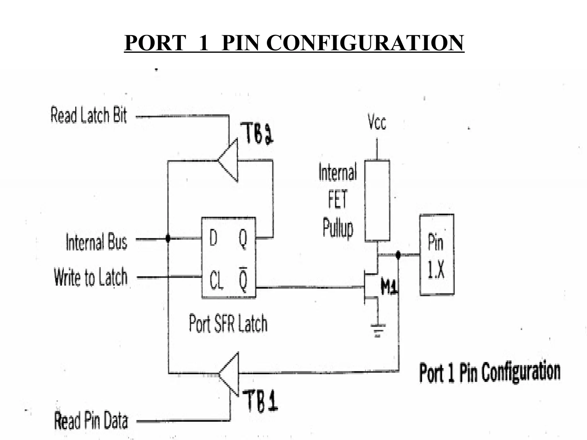
• Input Port:To use each pin as an input pin , we must write ‘1’ (LOGIC HIGH) to that bit i.e., 1) Writing ‘1’ to Port-1 pin , the D flip flop output is high i.e., Q=1 & Q=0. 2) Since Q = 0 & is connected to the FET’s gate M1 ,thus turning OFF the FET. 3) When M1 is OFF , it acts like open circuit (it blocks any path to the ground) thus input signal is directed to the tristate buffer TB1. • Output Port:To use each pin as an output pin , we must write ‘0’ (LOGIC ZERO) to that bit i.e., 1)Writing ‘0’ to Port-1 pin , the D flip flop output is low i.e., Q=0 & Q=1. 2)Since Q = 1 & is directly connected to the FET’s gate M1 ,thus turning ON the FET. 3) When M1 is ON , it acts like short circuit & thus Port-1 pin is connected to the ground. Therefore any attempt to read the input pin will always get the LOW ground signal regardless of the status of the input pin. NOTE • PORT-1 address is 90H • PORT-1 pins do not have any dual function. It has only the input output functions. • PORT-1 pins has internal pull-up resistors.
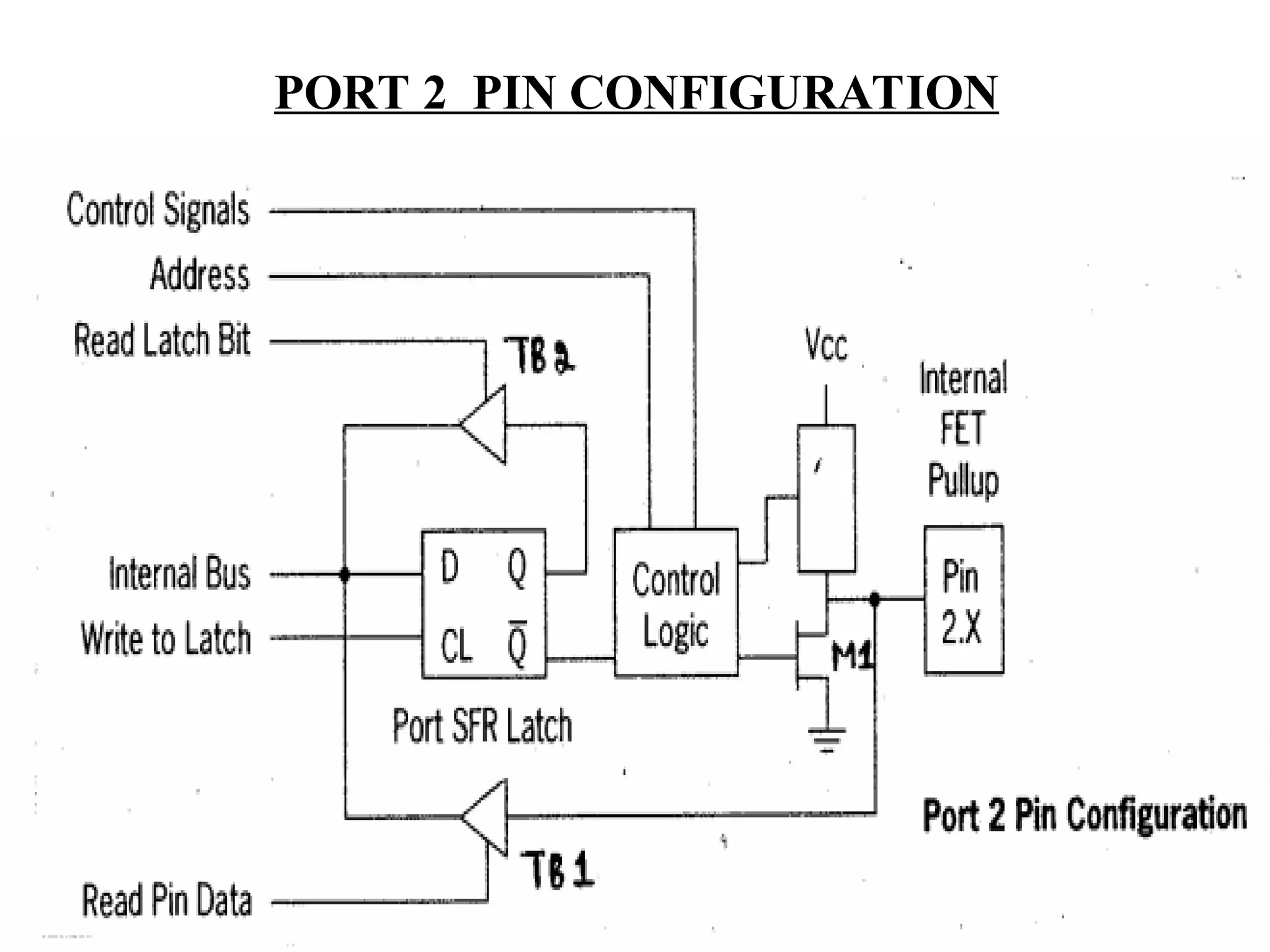
• Input Port:To use each pin as an input pin , we must write ‘1’ (LOGIC HIGH) to that bit i.e., 1) Writing ‘1’ to Port-2 pin , the D flip flop output is high i.e., Q=1 & Q=0. 2) Since Q = 0 & is connected to the FET’s gate M1 ,thus turning OFF the FET. 3) When M1 is OFF , it acts like open circuit (it blocks any path to the ground) thus input signal is directed to the tristate buffer TB1. • Output Port:To use each pin as an output pin , we must write ‘0’ (LOGIC ZERO) to that bit i.e., 1)Writing ‘0’ to Port-2 pin , the D flip flop output is low i.e., Q=0 & Q=1. 2)Since Q = 1 & is directly connected to the FET’s gate M1 ,thus turning ON the FET. 3) When M1 is ON , it acts like short circuit & thus Port-2 pin is connected to the ground. Therefore any attempt to read the input pin will always get the LOW ground signal regardless of the status of the input pin. NOTE • PORT-2 address is A0H • PORT-2 pins have dual function. PORT-2 pins are used to carry the higher order address A8-A15 during the external memory access & also as input output pins. • PORT-2 pins have internal pull-up resistors.
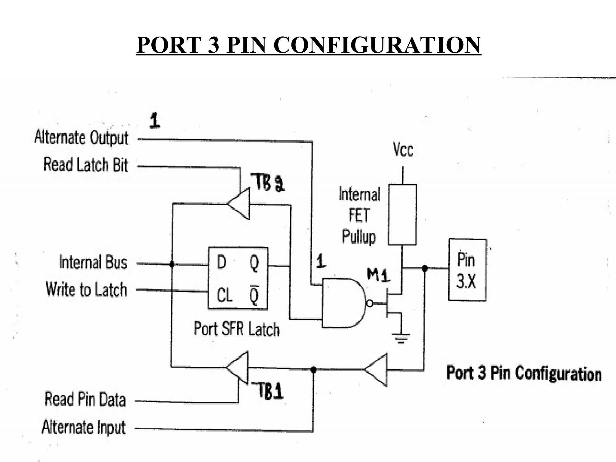
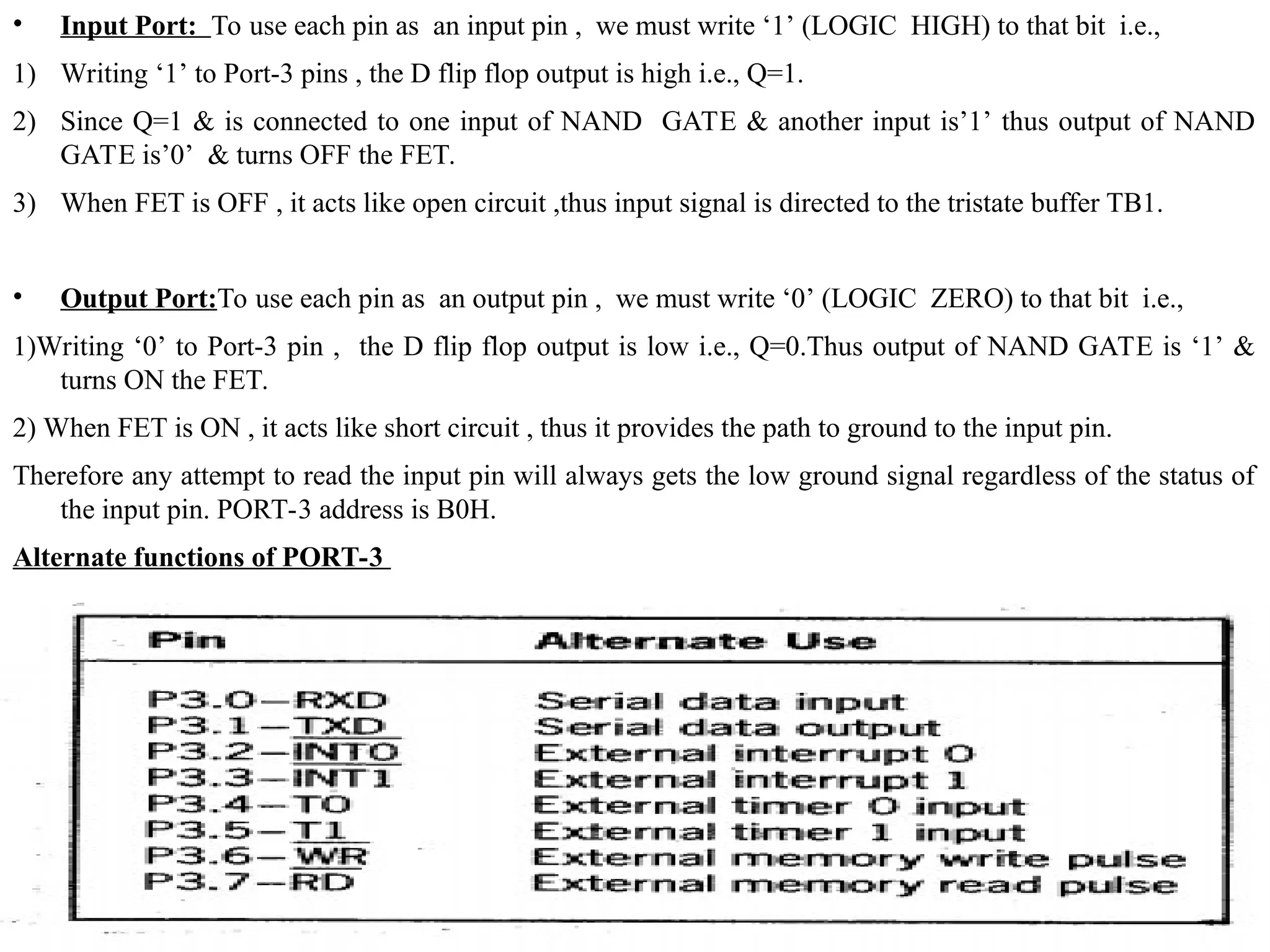
• Input Port:To use each pin as an input pin , we must write ‘1’ (LOGIC HIGH) to that bit i.e., 1) Writing ‘1’ to Port-3 pins , the D flip flop output is high i.e., Q=1. 2) Since Q=1 & is connected to one input of NAND GATE & another input is’1’ thus output of NAND GATE is’0’ & turns OFF the FET. 3) When FET is OFF , it acts like open circuit ,thus input signal is directed to the tristate buffer TB1. • Output Port:To use each pin as an output pin , we must write ‘0’ (LOGIC ZERO) to that bit i.e., 1)Writing ‘0’ to Port-3 pin , the D flip flop output is low i.e., Q=0.Thus output of NAND GATE is ‘1’ & turns ON the FET. 2) When FET is ON , it acts like short circuit , thus it provides the path to ground to the input pin. Therefore any attempt to read the input pin will always gets the low ground signal regardless of the status of the input pin. PORT-3 address is B0H. Alternate functions of PORT-3
![FEATURES OF 8051 MICROCONTROLLER 1) 8 bit CPU 2) On chip clock oscillator 3) 4K bytes of internal program memory (code memory ) [ROM] 4) 128 bytes of internal data memory [RAM] 5) 64K bytes of external program memory address space 6) 64K bytes of external data memory space 7) 32 bidirectional I/O lines 8) Two 16 bit Timer/ Counter : T0, T1 9) Full duplex serial data receiver/ transmitter 10)Four register banks with 8 registers in each bank 11)Sixteen bit Program Counter (PC) and Data pointer(DPTR) 12)8 bit Program Status Word (PSW) and 8 bit Stack pointer 13)Two external and three internal interrupt sources](https://image.slidesharecdn.com/mc-module-1-250723060040-88660a66/75/MICROCONTROLLER-MODULE-1-PPT-Includes-basics-of-microcontroller-applications-memory-interfacing-etc-18-2048.jpg)