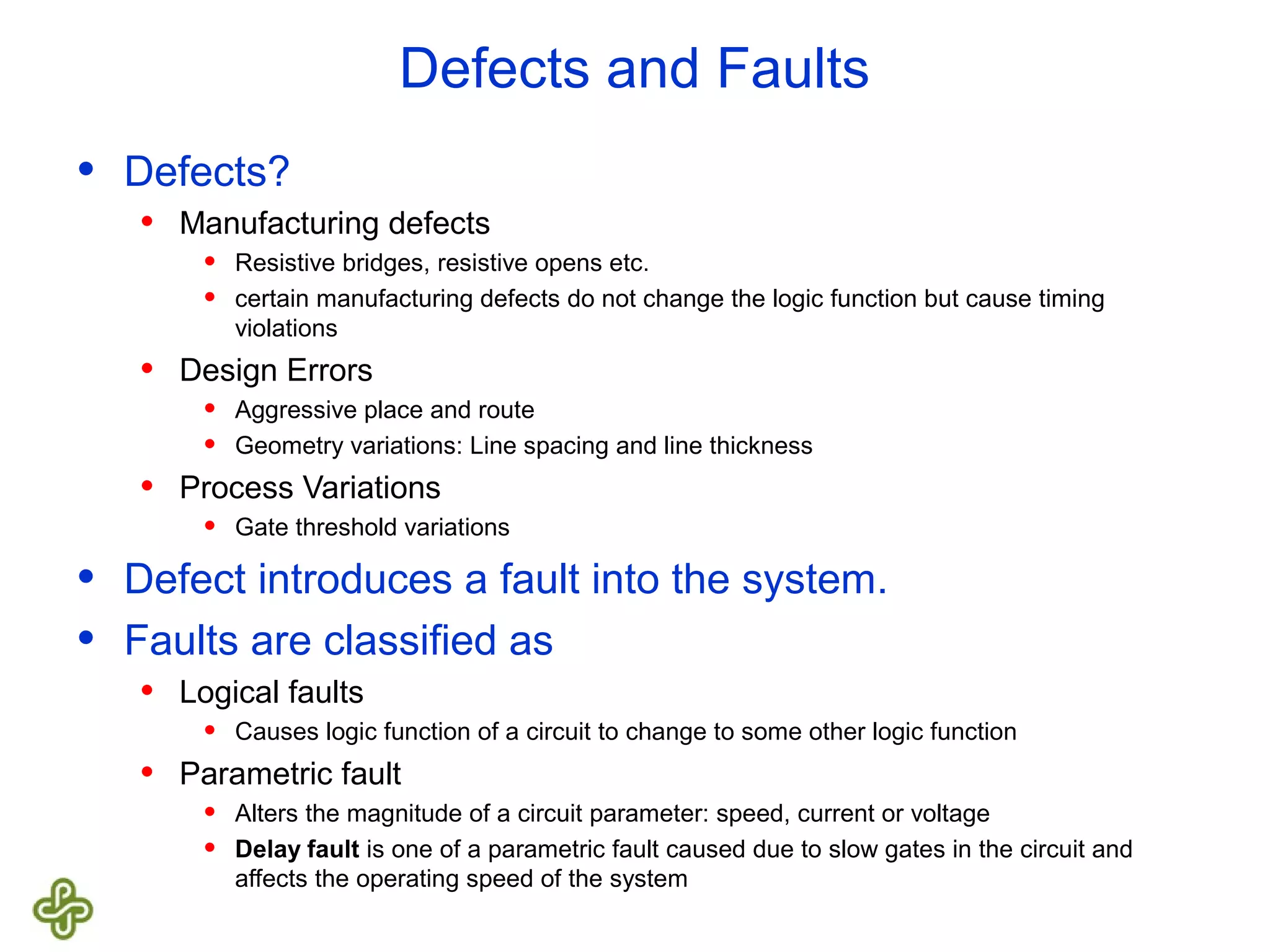
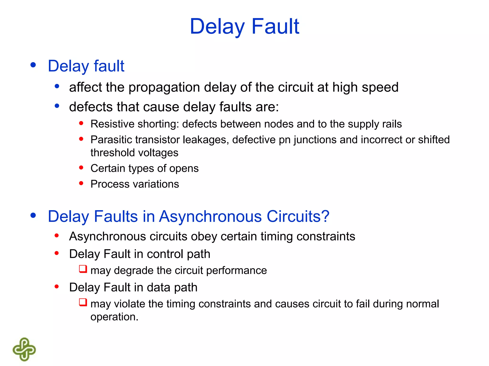
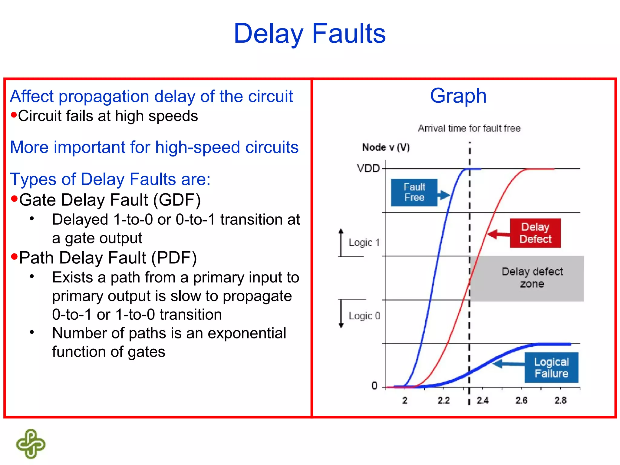
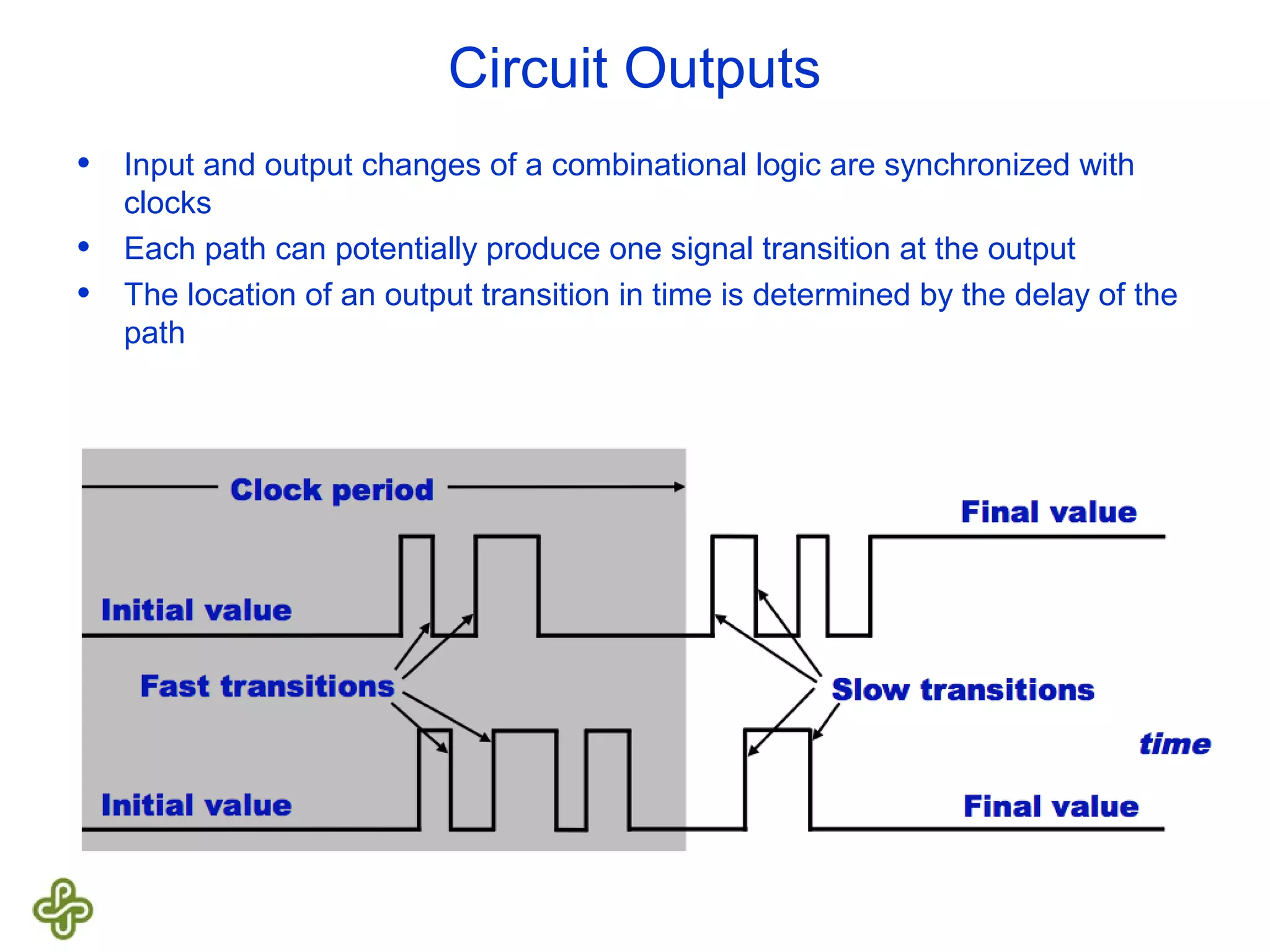
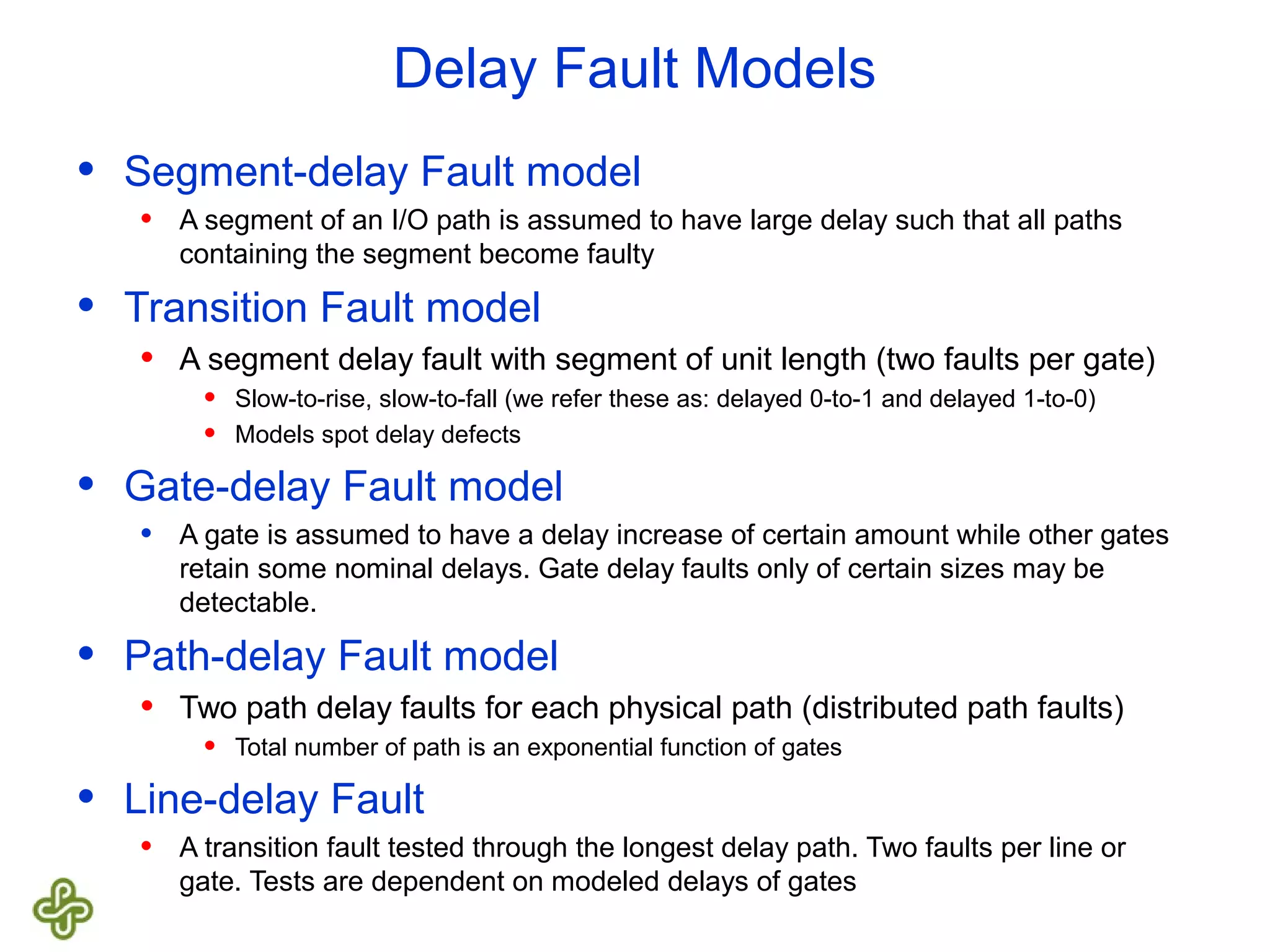
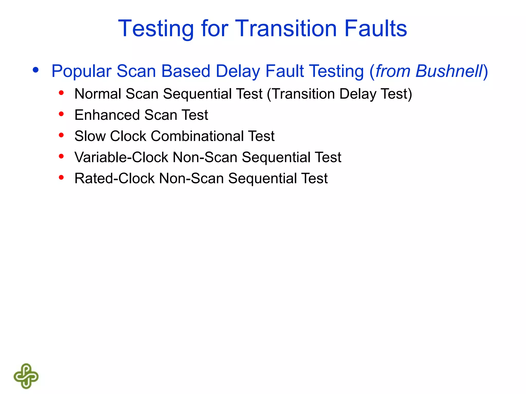
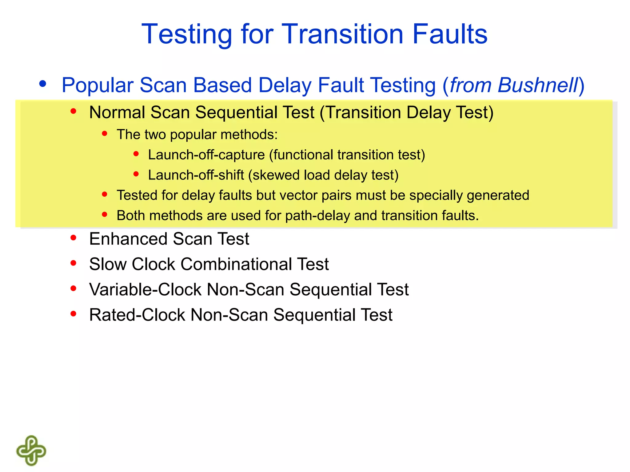
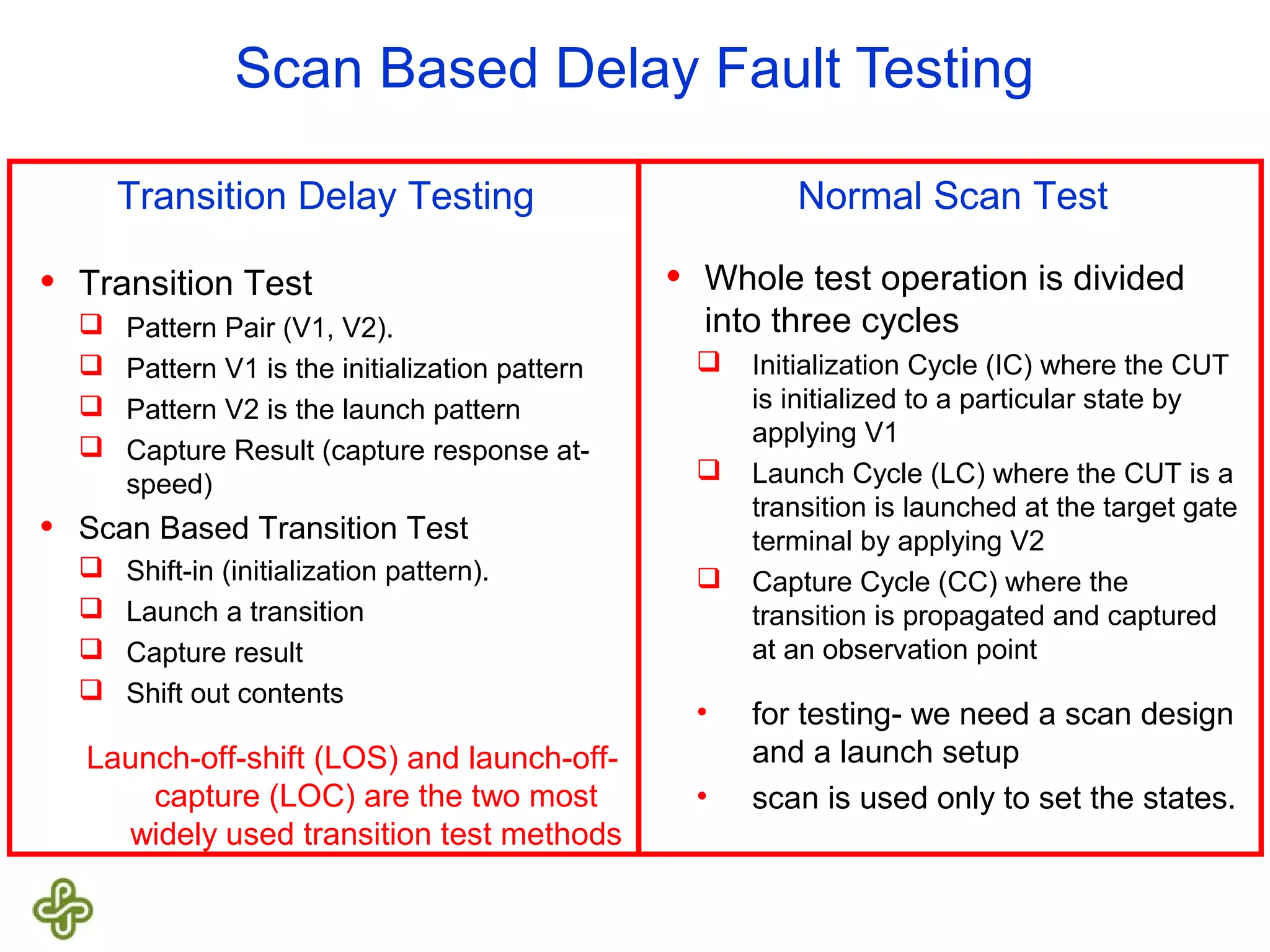
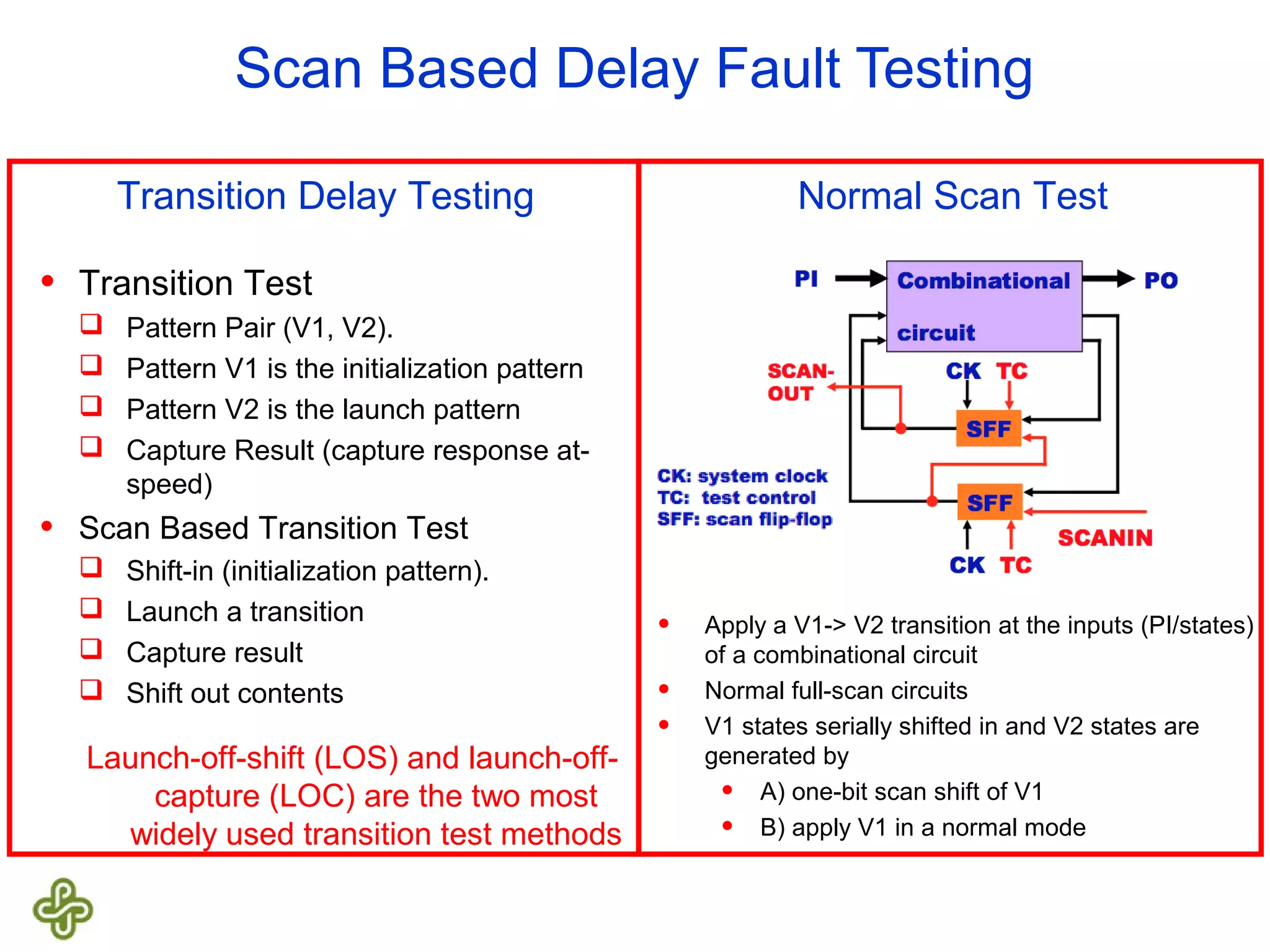
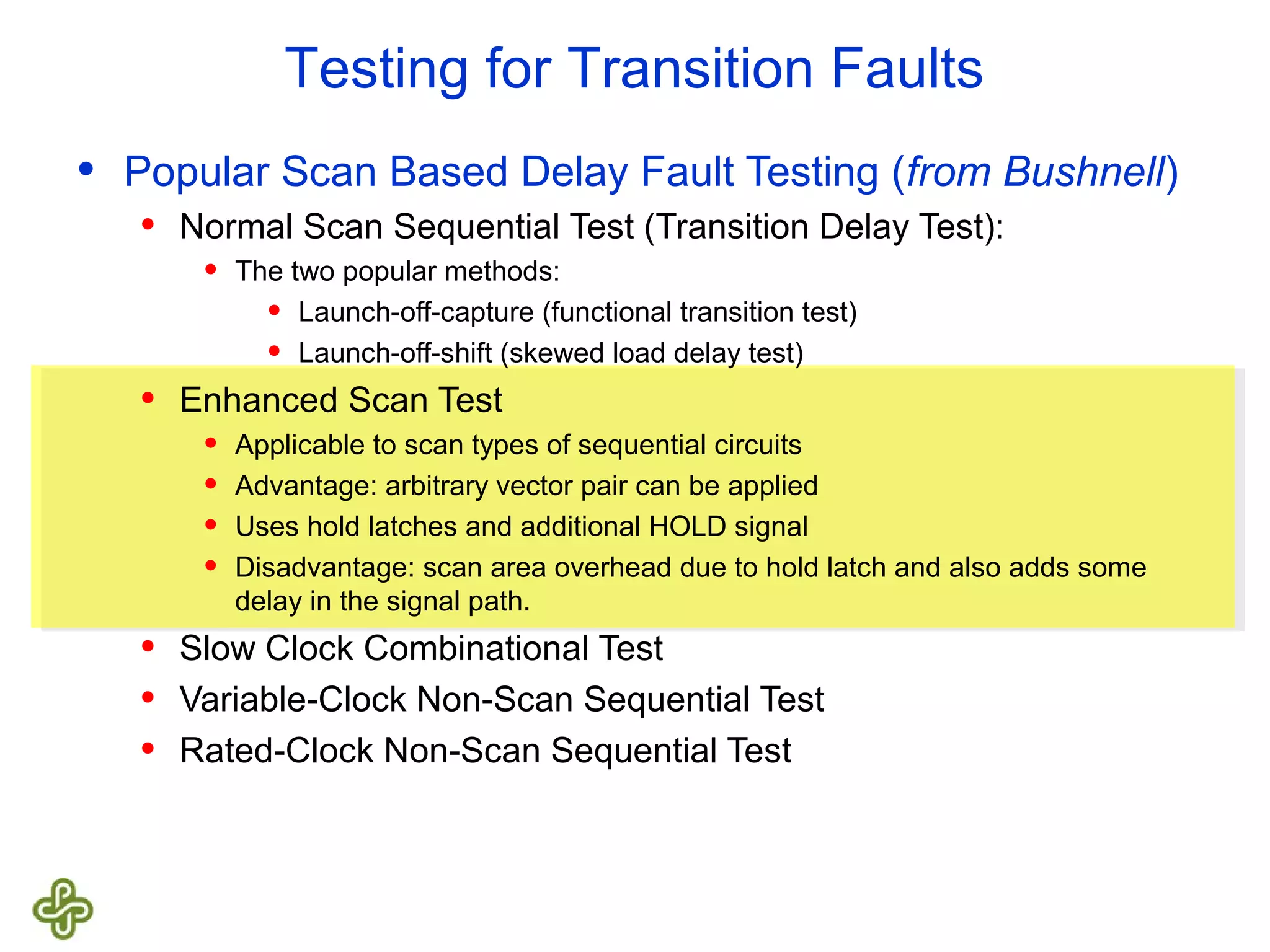
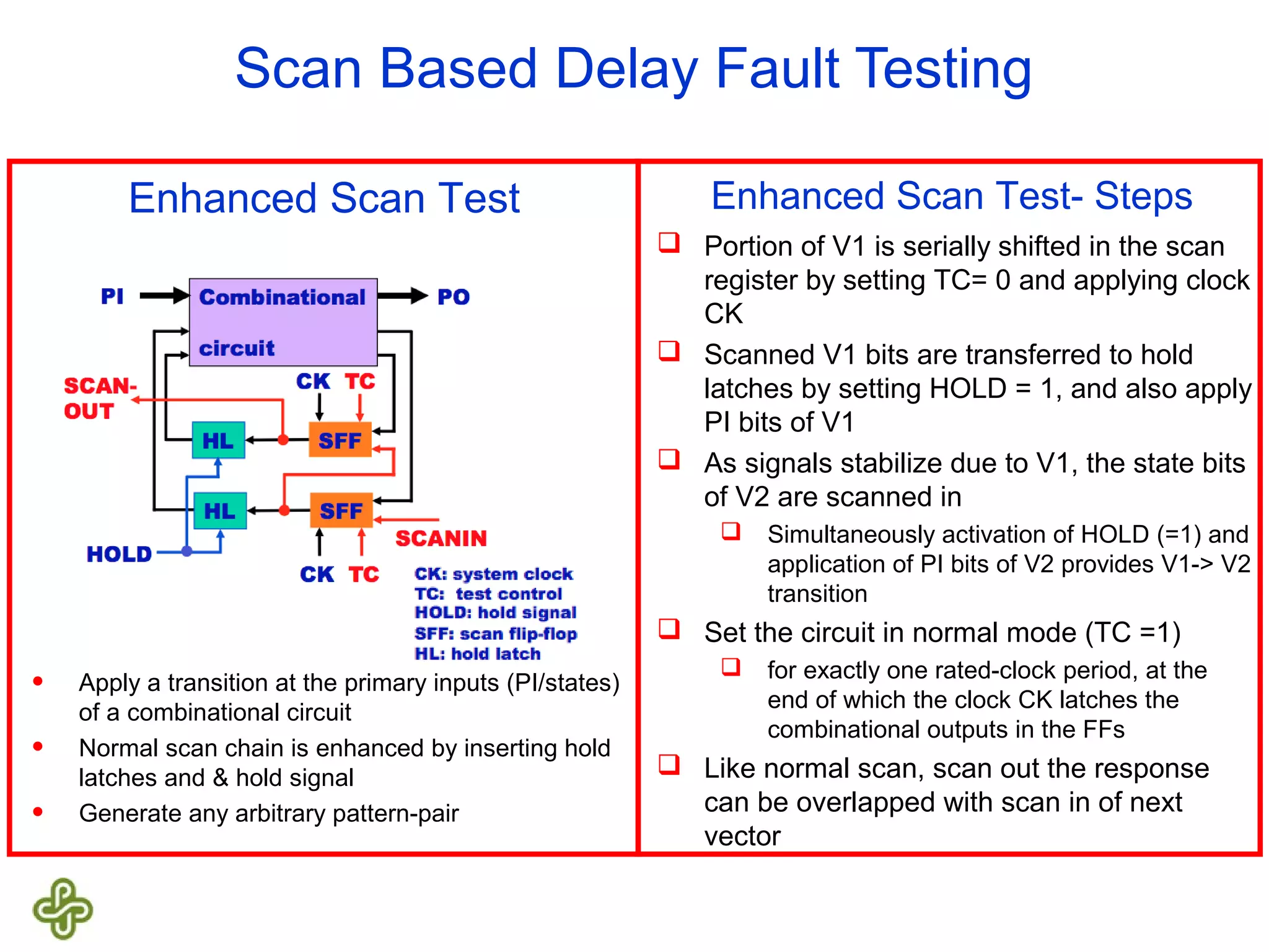
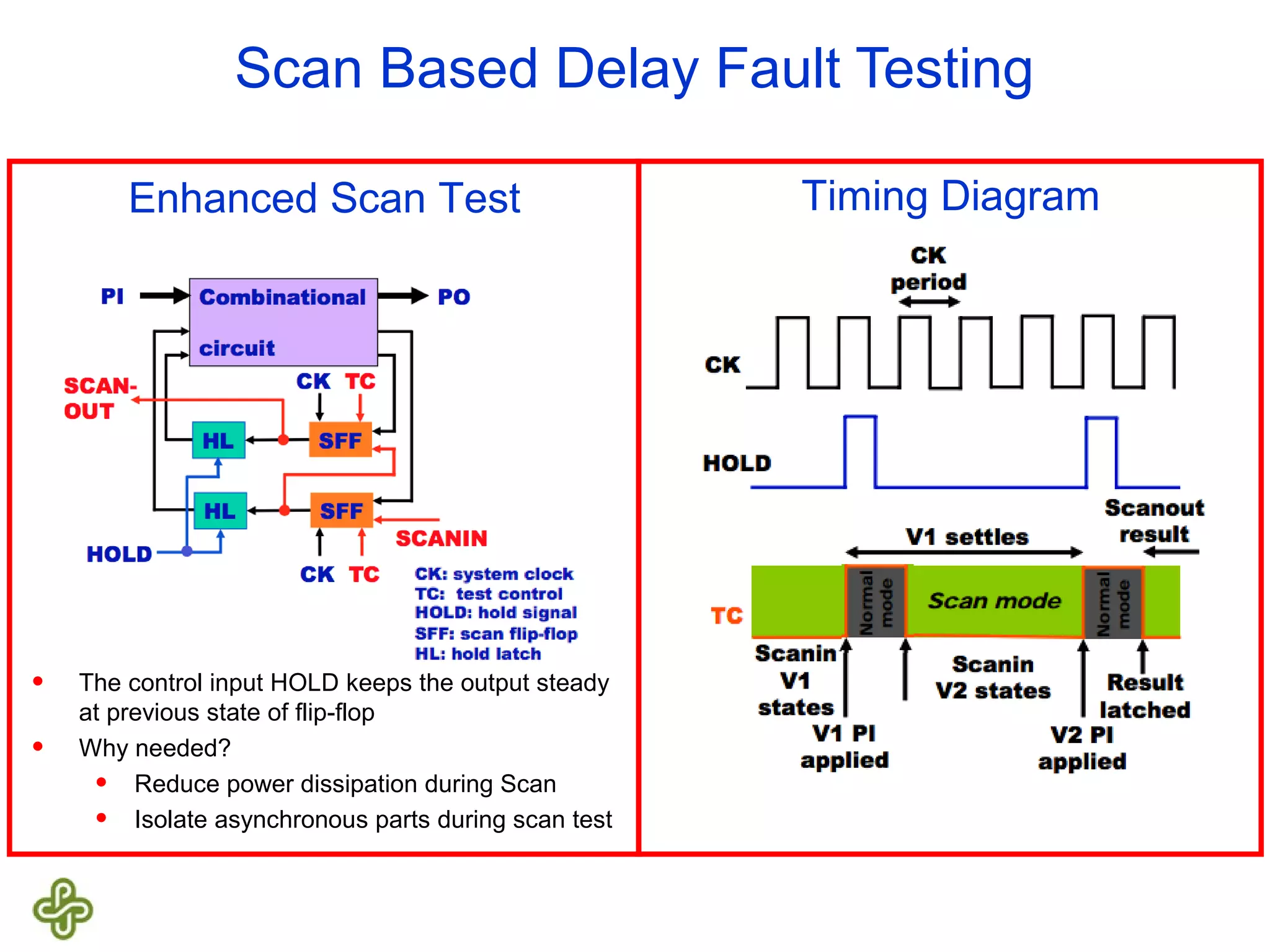
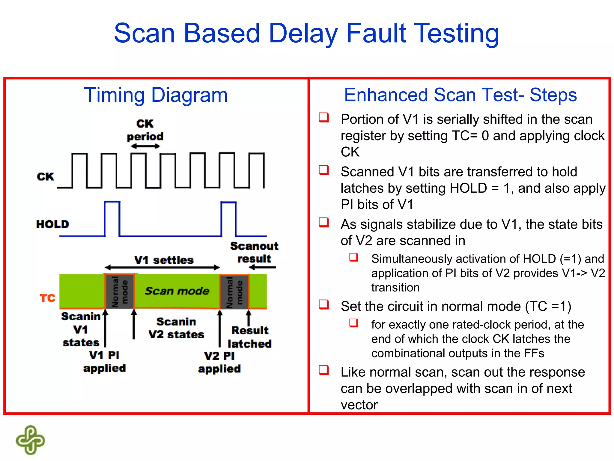
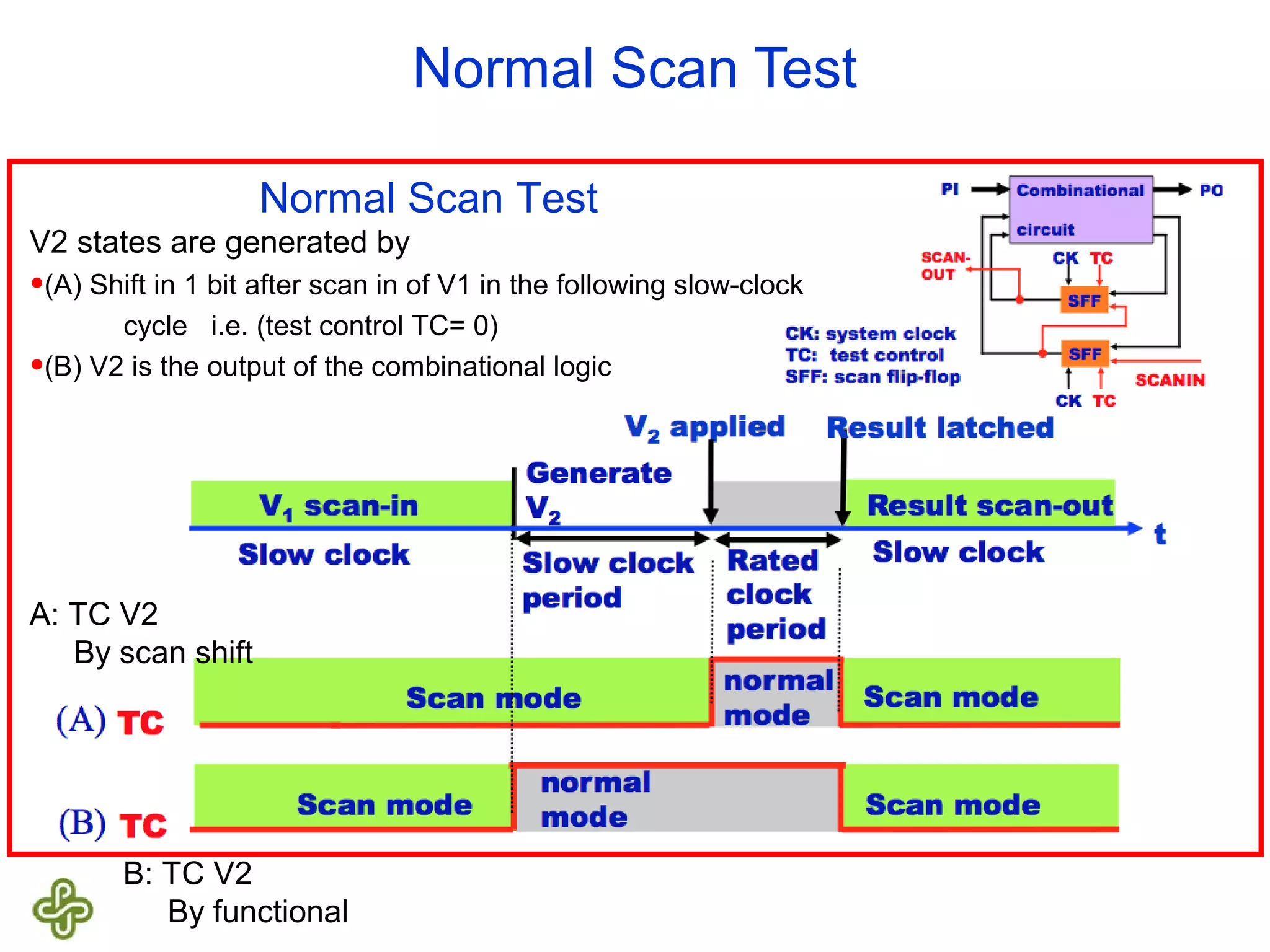
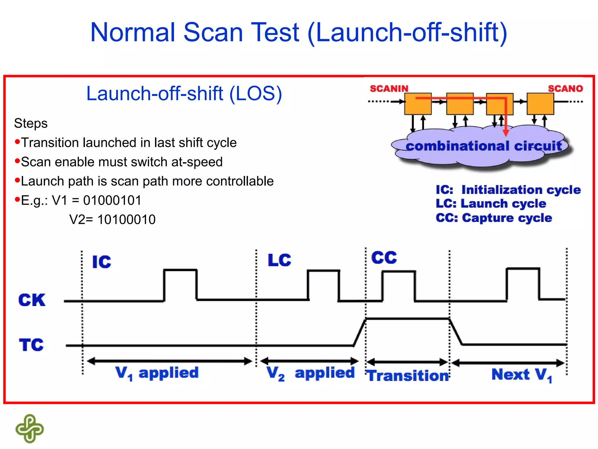
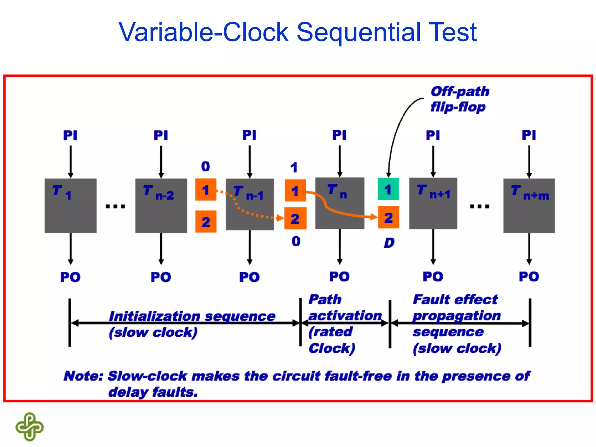
Transition Fault Testing – Delay fault models Swetha Mettala Gilla Maseeh College of Engineering and Computer Science Portland State University Summer 2015 slide 1 of 63
Book References [1] M. L. Bushnell and V. D. Agrawal “Chapter 12- Delay Test, Book -Essentials of Electronic Testing for Digital, Memory, and Mixed-Signal VLSI Circuits,” Springer, 2005. [2] M. Abramovici et al., “Digital Systems Testing and Testable Design,” IEEE 2009. [3] A. Krstic and K.T Cheng, “Delay Fault Testing for VLSI Circuits,” IEEE 1998. [4] S. K. Goel, “Testing for Small-Delay Defects in Nanoscale CMOS Integrated Circuits,” Taylor and Francis Group, 2013. [5] M. Tehranipoor et al., “Chapter 2: Delay Test, Book: Test and Diagnosis for Small-Delay Defects,” Springer, 2011.
Defects and Faults • Defects? • Manufacturing defects • Resistive bridges, resistive opens etc. • certain manufacturing defects do not change the logic function but cause timing violations • Design Errors • Aggressive place and route • Geometry variations: Line spacing and line thickness • Process Variations • Gate threshold variations • Defect introduces a fault into the system. • Faults are classified as • Logical faults • Causes logic function of a circuit to change to some other logic function • Parametric fault • Alters the magnitude of a circuit parameter: speed, current or voltage • Delay fault is one of a parametric fault caused due to slow gates in the circuit and affects the operating speed of the system
Delay Fault • Delay fault • affect the propagation delay of the circuit at high speed • defects that cause delay faults are: • Resistive shorting: defects between nodes and to the supply rails • Parasitic transistor leakages, defective pn junctions and incorrect or shifted threshold voltages • Certain types of opens • Process variations • Delay Faults in Asynchronous Circuits? • Asynchronous circuits obey certain timing constraints • Delay Fault in control path  may degrade the circuit performance • Delay Fault in data path  may violate the timing constraints and causes circuit to fail during normal operation.
Delay Faults Affect propagation delay of the circuit •Circuit fails at high speeds More important for high-speed circuits Types of Delay Faults are: •Gate Delay Fault (GDF) • Delayed 1-to-0 or 0-to-1 transition at a gate output •Path Delay Fault (PDF) • Exists a path from a primary input to primary output is slow to propagate 0-to-1 or 1-to-0 transition • Number of paths is an exponential function of gates Graph
Delay Fault Testing • Fault Models • Stuck-at fault test covers • Shorts and opens • Resistive shorts – Not covered • Delay fault test covers • Resistive opens and coupling faults • Resistive power supply lines • Process variations • Delay Fault Testing • Propagation delay of all paths in a circuit must be less than clock period for correct operation • Functional tests applied at operational speed of circuit are often used for delay faults • Scan based stuck-at tests are often applied at speed • However, functional and stuck-at testing even if done at-speed do not specifically target delay faults
Transition Faults • Detection • Testing for gate delay faults require accounting for delay defect size. Ex: if the defect size at a circuit lead r is less than the slack of r, the fault may not be detected. • Slack of a circuit line is the difference between the period of the functional clock and the max delay of all paths through r. • Types of Gate Delay Faults • Gross gate delay fault (G-GDF): one gate delay defect size is greater than the system clock period • DFs in all paths going through faulty gate, hence catastrophic • Also called as transition fault • Small GDF (S-GDF): delay defect size is smaller than system clock period • Detectable if causes Path Delay Fault in at least one path through the gate We want to focus on Gross gate delay fault i.e. Transition fault
• All input transitions occur at the same time in the figure below • The position of each output transition depends upon the delay of some input to output combinational path • The right edge of the output transition(red shaded region) is determined by the last transition • Delay of the longest combinational path activated by the current input vector • The delay of critical paths determines the smallest clock period at which the circuit can function correctly. Digital Circuit Timing
Circuit Delays • Switching or inertial delay • Interval between input change and output change of a gate • Depends on input capacitance, device (transistor) characteristics and output capacitance of gate • Also depends on input rise or fall times and states of other inputs (second- order effects) • Approximation: fixed rise and fall delays (or min-max range delay) for gate output • Propagation delay or interconnect delay • Is the time a transition takes to travel between gates • Depends on transmission line effects (distributed R,L, C parameters, length, loading) of routing paths • Approximation: modeled as lumped delays for gate inputs
Circuit Outputs • Input and output changes of a combinational logic are synchronized with clocks • Each path can potentially produce one signal transition at the output • The location of an output transition in time is determined by the delay of the path
Delay Fault Models • Segment-delay Fault model • A segment of an I/O path is assumed to have large delay such that all paths containing the segment become faulty • Transition Fault model • A segment delay fault with segment of unit length (two faults per gate) • Slow-to-rise, slow-to-fall (we refer these as: delayed 0-to-1 and delayed 1-to-0) • Models spot delay defects • Gate-delay Fault model • A gate is assumed to have a delay increase of certain amount while other gates retain some nominal delays. Gate delay faults only of certain sizes may be detectable. • Path-delay Fault model • Two path delay faults for each physical path (distributed path faults) • Total number of path is an exponential function of gates • Line-delay Fault • A transition fault tested through the longest delay path. Two faults per line or gate. Tests are dependent on modeled delays of gates
Transition Delay Fault • Transition fault (or Gross Gate Delay fault) • Even though the circuit doesn’t have a logical defect, it may have some physical defect such as a process variation and that creates a large enough gate delay to cause problems • Transition Fault model • Assumes that the delay fault affects only one gate in the circuit • Assumes the logic function of circuit under test (CUT) is error-free • Types of faults: delayed 0-to-1 & delayed 1-to-0  Fault at any node means the effect of any transition from 0 to 1 for delayed high (or 1 to 0 for delayed low) will not reach primary output within the stipulated time  extra delay (delay above the nominal delay) caused by the fault is assumed to be large enough to prevent the transition from reaching primary output at the time of observation • Advantages • the number of faults in the circuit increase linearly with the number of gates • Practically used: stuck-at fault CAD tools with minor modifications [Goel2013][Waicukauski1987]
Testing for Transition Faults • Popular Scan Based Delay Fault Testing (from Bushnell) • Normal Scan Sequential Test (Transition Delay Test) • Enhanced Scan Test • Slow Clock Combinational Test • Variable-Clock Non-Scan Sequential Test • Rated-Clock Non-Scan Sequential Test
Testing for Transition Faults • Popular Scan Based Delay Fault Testing (from Bushnell) • Normal Scan Sequential Test (Transition Delay Test) • The two popular methods: • Launch-off-capture (functional transition test) • Launch-off-shift (skewed load delay test) • Tested for delay faults but vector pairs must be specially generated • Both methods are used for path-delay and transition faults. • Enhanced Scan Test • Slow Clock Combinational Test • Variable-Clock Non-Scan Sequential Test • Rated-Clock Non-Scan Sequential Test
Scan Based Delay Fault Testing Transition Delay Testing Normal Scan Test • Whole test operation is divided into three cycles  Initialization Cycle (IC) where the CUT is initialized to a particular state by applying V1  Launch Cycle (LC) where the CUT is a transition is launched at the target gate terminal by applying V2  Capture Cycle (CC) where the transition is propagated and captured at an observation point • for testing- we need a scan design and a launch setup • scan is used only to set the states. • Transition Test  Pattern Pair (V1, V2).  Pattern V1 is the initialization pattern  Pattern V2 is the launch pattern  Capture Result (capture response at- speed) • Scan Based Transition Test  Shift-in (initialization pattern).  Launch a transition  Capture result  Shift out contents Launch-off-shift (LOS) and launch-off- capture (LOC) are the two most widely used transition test methods
Scan Based Delay Fault Testing Transition Delay Testing • Transition Test  Pattern Pair (V1, V2).  Pattern V1 is the initialization pattern  Pattern V2 is the launch pattern  Capture Result (capture response at- speed) • Scan Based Transition Test  Shift-in (initialization pattern).  Launch a transition  Capture result  Shift out contents Launch-off-shift (LOS) and launch-off- capture (LOC) are the two most widely used transition test methods Normal Scan Test • Apply a V1-> V2 transition at the inputs (PI/states) of a combinational circuit • Normal full-scan circuits • V1 states serially shifted in and V2 states are generated by • A) one-bit scan shift of V1 • B) apply V1 in a normal mode
Testing for Transition Faults • Popular Scan Based Delay Fault Testing (from Bushnell) • Normal Scan Sequential Test (Transition Delay Test): • The two popular methods: • Launch-off-capture (functional transition test) • Launch-off-shift (skewed load delay test) • Enhanced Scan Test • Applicable to scan types of sequential circuits • Advantage: arbitrary vector pair can be applied • Uses hold latches and additional HOLD signal • Disadvantage: scan area overhead due to hold latch and also adds some delay in the signal path. • Slow Clock Combinational Test • Variable-Clock Non-Scan Sequential Test • Rated-Clock Non-Scan Sequential Test
Scan Based Delay Fault Testing Enhanced Scan Test • Apply a transition at the primary inputs (PI/states) of a combinational circuit • Normal scan chain is enhanced by inserting hold latches and & hold signal • Generate any arbitrary pattern-pair Enhanced Scan Test- Steps  Portion of V1 is serially shifted in the scan register by setting TC= 0 and applying clock CK  Scanned V1 bits are transferred to hold latches by setting HOLD = 1, and also apply PI bits of V1  As signals stabilize due to V1, the state bits of V2 are scanned in  Simultaneously activation of HOLD (=1) and application of PI bits of V2 provides V1-> V2 transition  Set the circuit in normal mode (TC =1)  for exactly one rated-clock period, at the end of which the clock CK latches the combinational outputs in the FFs  Like normal scan, scan out the response can be overlapped with scan in of next vector
Scan Based Delay Fault Testing Enhanced Scan Test Timing Diagram • The control input HOLD keeps the output steady at previous state of flip-flop • Why needed? • Reduce power dissipation during Scan • Isolate asynchronous parts during scan test
Scan Based Delay Fault Testing Enhanced Scan Test- Steps  Portion of V1 is serially shifted in the scan register by setting TC= 0 and applying clock CK  Scanned V1 bits are transferred to hold latches by setting HOLD = 1, and also apply PI bits of V1  As signals stabilize due to V1, the state bits of V2 are scanned in  Simultaneously activation of HOLD (=1) and application of PI bits of V2 provides V1-> V2 transition  Set the circuit in normal mode (TC =1)  for exactly one rated-clock period, at the end of which the clock CK latches the combinational outputs in the FFs  Like normal scan, scan out the response can be overlapped with scan in of next vector Timing Diagram
Normal Scan Test Normal Scan Test V2 states are generated by •(A) Shift in 1 bit after scan in of V1 in the following slow-clock cycle i.e. (test control TC= 0) •(B) V2 is the output of the combinational logic A: TC V2 By scan shift B: TC V2 By functional
Normal Scan Test (Launch-off-shift) Launch-off-shift (LOS) Steps •Transition launched in last shift cycle •Scan enable must switch at-speed •Launch path is scan path more controllable •E.g.: V1 = 01000101 V2= 10100010
Normal Scan Test (Launch-off-capture) Launch-off-capture (LOC) Steps •Transition launched from functional path •Scan enable doesn’t have to switch at-speed •Functional launch path - less controllable
Testing for Transition Faults • Popular Scan Based Delay Fault Testing (from Bushnell) • Normal Scan Sequential Test (Transition Delay Test) • The two popular methods: • Launch-off-capture (functional transition test) • Launch-off-shift (skewed load delay test) • Enhanced Scan Test • Applicable to scan types of sequential circuits • Slow Clock Combinational Test • Applicable to combinational circuits or to those sequential circuits that are internally combinational with flip-flops only at PIs and POs • This method is useful when ATE cannot apply the vectors at rated speed • Variable-Clock Non-Scan Sequential Test • Rated-Clock Non-Scan Sequential Test
Slow-Clock Test
Testing for Transition Faults • Popular Scan Based Delay Fault Testing (from Bushnell) • Normal Scan Sequential Test (Transition Delay Test): • The two popular methods: • Launch-off-capture (functional transition test) • Launch-off-shift (skewed load delay test) • Enhanced Scan Test • Applicable to scan types of sequential circuits • Slow Clock Combinational Test • Applicable to combinational circuits or to those sequential circuits that are internally combinational with flip-flops only at PIs and POs • Variable-Clock Non-Scan Sequential Test • Requires more than two vectors • Slow-clock prevents the delays in the circuit interfering with detection of the target fault • Since rated clock is used, other path delays can also affect the signals and the state FFs. • Rated-Clock Non-Scan Sequential Test
Variable-Clock Sequential Test
Testing for Transition Faults • Popular Scan Based Delay Fault Testing (from Bushnell) • Normal Scan Sequential Test (Transition Delay Test): • The two popular methods: • Launch-off-capture (functional transition test) • Launch-off-shift (skewed load delay test) • Enhanced Scan Test • Applicable to scan types of sequential circuits • Slow Clock Combinational Test • Applicable to combinational circuits or to those sequential circuits that are internally combinational with flip-flops only at PIs and Pos • Variable-Clock Non-Scan Sequential Test • Requires more than two vectors • Rated-Clock Non-Scan Sequential Test • Most natural form of test. All vectors are applied at rated speed. A target delay fault can be activated several times • If robust detection is desired, one must consider all delay combinations that are potentially possible : PS I don’t have any example slide at the moment
Other References [1] N. Ahmed et al, “Enhanced Launch-off-capture Transition Fault Testing,” IEC, pp. 279–289, 2005. [2] M. Roncken, “Defect-Oriented Testability for Asynchronous ICs,” In Proc. IEEE, vol. 87, no. 2, pp. 363–375, Feb.1999. [3] D. Vasudevan, “Automatic Test Pattern Generation for Asynchronous Circuits,” Dissertation, 2012. [4] S. Jayanthy et al, “Fuzzy Delay Model Based Fault Simulator for Crosstalk Delay Fault Test Generation in Asynchronous Sequential Circuits,” IAS, 2015. [5] M. Roncken et al, “Fsimac: A Fault Simulator for Asynchronous Sequential Circuits,” IEEE, 2000. [6] J. A. Waicukauski et al., “Transition Fault Simulation,” IEEE Design and Test, 1987.

01 Transition Fault Detection methods by Swetha

  • 1.
    Transition Fault Testing –Delay fault models Swetha Mettala Gilla Maseeh College of Engineering and Computer Science Portland State University Summer 2015 slide 1 of 63
  • 2.
    Book References [1] M.L. Bushnell and V. D. Agrawal “Chapter 12- Delay Test, Book -Essentials of Electronic Testing for Digital, Memory, and Mixed-Signal VLSI Circuits,” Springer, 2005. [2] M. Abramovici et al., “Digital Systems Testing and Testable Design,” IEEE 2009. [3] A. Krstic and K.T Cheng, “Delay Fault Testing for VLSI Circuits,” IEEE 1998. [4] S. K. Goel, “Testing for Small-Delay Defects in Nanoscale CMOS Integrated Circuits,” Taylor and Francis Group, 2013. [5] M. Tehranipoor et al., “Chapter 2: Delay Test, Book: Test and Diagnosis for Small-Delay Defects,” Springer, 2011.
  • 3.
    Defects and Faults •Defects? • Manufacturing defects • Resistive bridges, resistive opens etc. • certain manufacturing defects do not change the logic function but cause timing violations • Design Errors • Aggressive place and route • Geometry variations: Line spacing and line thickness • Process Variations • Gate threshold variations • Defect introduces a fault into the system. • Faults are classified as • Logical faults • Causes logic function of a circuit to change to some other logic function • Parametric fault • Alters the magnitude of a circuit parameter: speed, current or voltage • Delay fault is one of a parametric fault caused due to slow gates in the circuit and affects the operating speed of the system
  • 4.
    Delay Fault • Delayfault • affect the propagation delay of the circuit at high speed • defects that cause delay faults are: • Resistive shorting: defects between nodes and to the supply rails • Parasitic transistor leakages, defective pn junctions and incorrect or shifted threshold voltages • Certain types of opens • Process variations • Delay Faults in Asynchronous Circuits? • Asynchronous circuits obey certain timing constraints • Delay Fault in control path  may degrade the circuit performance • Delay Fault in data path  may violate the timing constraints and causes circuit to fail during normal operation.
  • 5.
    Delay Faults Affect propagationdelay of the circuit •Circuit fails at high speeds More important for high-speed circuits Types of Delay Faults are: •Gate Delay Fault (GDF) • Delayed 1-to-0 or 0-to-1 transition at a gate output •Path Delay Fault (PDF) • Exists a path from a primary input to primary output is slow to propagate 0-to-1 or 1-to-0 transition • Number of paths is an exponential function of gates Graph
  • 6.
    Delay Fault Testing •Fault Models • Stuck-at fault test covers • Shorts and opens • Resistive shorts – Not covered • Delay fault test covers • Resistive opens and coupling faults • Resistive power supply lines • Process variations • Delay Fault Testing • Propagation delay of all paths in a circuit must be less than clock period for correct operation • Functional tests applied at operational speed of circuit are often used for delay faults • Scan based stuck-at tests are often applied at speed • However, functional and stuck-at testing even if done at-speed do not specifically target delay faults
  • 7.
    Transition Faults • Detection •Testing for gate delay faults require accounting for delay defect size. Ex: if the defect size at a circuit lead r is less than the slack of r, the fault may not be detected. • Slack of a circuit line is the difference between the period of the functional clock and the max delay of all paths through r. • Types of Gate Delay Faults • Gross gate delay fault (G-GDF): one gate delay defect size is greater than the system clock period • DFs in all paths going through faulty gate, hence catastrophic • Also called as transition fault • Small GDF (S-GDF): delay defect size is smaller than system clock period • Detectable if causes Path Delay Fault in at least one path through the gate We want to focus on Gross gate delay fault i.e. Transition fault
  • 8.
    • All inputtransitions occur at the same time in the figure below • The position of each output transition depends upon the delay of some input to output combinational path • The right edge of the output transition(red shaded region) is determined by the last transition • Delay of the longest combinational path activated by the current input vector • The delay of critical paths determines the smallest clock period at which the circuit can function correctly. Digital Circuit Timing
  • 9.
    Circuit Delays • Switchingor inertial delay • Interval between input change and output change of a gate • Depends on input capacitance, device (transistor) characteristics and output capacitance of gate • Also depends on input rise or fall times and states of other inputs (second- order effects) • Approximation: fixed rise and fall delays (or min-max range delay) for gate output • Propagation delay or interconnect delay • Is the time a transition takes to travel between gates • Depends on transmission line effects (distributed R,L, C parameters, length, loading) of routing paths • Approximation: modeled as lumped delays for gate inputs
  • 10.
    Circuit Outputs • Inputand output changes of a combinational logic are synchronized with clocks • Each path can potentially produce one signal transition at the output • The location of an output transition in time is determined by the delay of the path
  • 11.
    Delay Fault Models •Segment-delay Fault model • A segment of an I/O path is assumed to have large delay such that all paths containing the segment become faulty • Transition Fault model • A segment delay fault with segment of unit length (two faults per gate) • Slow-to-rise, slow-to-fall (we refer these as: delayed 0-to-1 and delayed 1-to-0) • Models spot delay defects • Gate-delay Fault model • A gate is assumed to have a delay increase of certain amount while other gates retain some nominal delays. Gate delay faults only of certain sizes may be detectable. • Path-delay Fault model • Two path delay faults for each physical path (distributed path faults) • Total number of path is an exponential function of gates • Line-delay Fault • A transition fault tested through the longest delay path. Two faults per line or gate. Tests are dependent on modeled delays of gates
  • 12.
    Transition Delay Fault •Transition fault (or Gross Gate Delay fault) • Even though the circuit doesn’t have a logical defect, it may have some physical defect such as a process variation and that creates a large enough gate delay to cause problems • Transition Fault model • Assumes that the delay fault affects only one gate in the circuit • Assumes the logic function of circuit under test (CUT) is error-free • Types of faults: delayed 0-to-1 & delayed 1-to-0  Fault at any node means the effect of any transition from 0 to 1 for delayed high (or 1 to 0 for delayed low) will not reach primary output within the stipulated time  extra delay (delay above the nominal delay) caused by the fault is assumed to be large enough to prevent the transition from reaching primary output at the time of observation • Advantages • the number of faults in the circuit increase linearly with the number of gates • Practically used: stuck-at fault CAD tools with minor modifications [Goel2013][Waicukauski1987]
  • 13.
    Testing for TransitionFaults • Popular Scan Based Delay Fault Testing (from Bushnell) • Normal Scan Sequential Test (Transition Delay Test) • Enhanced Scan Test • Slow Clock Combinational Test • Variable-Clock Non-Scan Sequential Test • Rated-Clock Non-Scan Sequential Test
  • 14.
    Testing for TransitionFaults • Popular Scan Based Delay Fault Testing (from Bushnell) • Normal Scan Sequential Test (Transition Delay Test) • The two popular methods: • Launch-off-capture (functional transition test) • Launch-off-shift (skewed load delay test) • Tested for delay faults but vector pairs must be specially generated • Both methods are used for path-delay and transition faults. • Enhanced Scan Test • Slow Clock Combinational Test • Variable-Clock Non-Scan Sequential Test • Rated-Clock Non-Scan Sequential Test
  • 15.
    Scan Based DelayFault Testing Transition Delay Testing Normal Scan Test • Whole test operation is divided into three cycles  Initialization Cycle (IC) where the CUT is initialized to a particular state by applying V1  Launch Cycle (LC) where the CUT is a transition is launched at the target gate terminal by applying V2  Capture Cycle (CC) where the transition is propagated and captured at an observation point • for testing- we need a scan design and a launch setup • scan is used only to set the states. • Transition Test  Pattern Pair (V1, V2).  Pattern V1 is the initialization pattern  Pattern V2 is the launch pattern  Capture Result (capture response at- speed) • Scan Based Transition Test  Shift-in (initialization pattern).  Launch a transition  Capture result  Shift out contents Launch-off-shift (LOS) and launch-off- capture (LOC) are the two most widely used transition test methods
  • 16.
    Scan Based DelayFault Testing Transition Delay Testing • Transition Test  Pattern Pair (V1, V2).  Pattern V1 is the initialization pattern  Pattern V2 is the launch pattern  Capture Result (capture response at- speed) • Scan Based Transition Test  Shift-in (initialization pattern).  Launch a transition  Capture result  Shift out contents Launch-off-shift (LOS) and launch-off- capture (LOC) are the two most widely used transition test methods Normal Scan Test • Apply a V1-> V2 transition at the inputs (PI/states) of a combinational circuit • Normal full-scan circuits • V1 states serially shifted in and V2 states are generated by • A) one-bit scan shift of V1 • B) apply V1 in a normal mode
  • 17.
    Testing for TransitionFaults • Popular Scan Based Delay Fault Testing (from Bushnell) • Normal Scan Sequential Test (Transition Delay Test): • The two popular methods: • Launch-off-capture (functional transition test) • Launch-off-shift (skewed load delay test) • Enhanced Scan Test • Applicable to scan types of sequential circuits • Advantage: arbitrary vector pair can be applied • Uses hold latches and additional HOLD signal • Disadvantage: scan area overhead due to hold latch and also adds some delay in the signal path. • Slow Clock Combinational Test • Variable-Clock Non-Scan Sequential Test • Rated-Clock Non-Scan Sequential Test
  • 18.
    Scan Based DelayFault Testing Enhanced Scan Test • Apply a transition at the primary inputs (PI/states) of a combinational circuit • Normal scan chain is enhanced by inserting hold latches and & hold signal • Generate any arbitrary pattern-pair Enhanced Scan Test- Steps  Portion of V1 is serially shifted in the scan register by setting TC= 0 and applying clock CK  Scanned V1 bits are transferred to hold latches by setting HOLD = 1, and also apply PI bits of V1  As signals stabilize due to V1, the state bits of V2 are scanned in  Simultaneously activation of HOLD (=1) and application of PI bits of V2 provides V1-> V2 transition  Set the circuit in normal mode (TC =1)  for exactly one rated-clock period, at the end of which the clock CK latches the combinational outputs in the FFs  Like normal scan, scan out the response can be overlapped with scan in of next vector
  • 19.
    Scan Based DelayFault Testing Enhanced Scan Test Timing Diagram • The control input HOLD keeps the output steady at previous state of flip-flop • Why needed? • Reduce power dissipation during Scan • Isolate asynchronous parts during scan test
  • 20.
    Scan Based DelayFault Testing Enhanced Scan Test- Steps  Portion of V1 is serially shifted in the scan register by setting TC= 0 and applying clock CK  Scanned V1 bits are transferred to hold latches by setting HOLD = 1, and also apply PI bits of V1  As signals stabilize due to V1, the state bits of V2 are scanned in  Simultaneously activation of HOLD (=1) and application of PI bits of V2 provides V1-> V2 transition  Set the circuit in normal mode (TC =1)  for exactly one rated-clock period, at the end of which the clock CK latches the combinational outputs in the FFs  Like normal scan, scan out the response can be overlapped with scan in of next vector Timing Diagram
  • 21.
    Normal Scan Test NormalScan Test V2 states are generated by •(A) Shift in 1 bit after scan in of V1 in the following slow-clock cycle i.e. (test control TC= 0) •(B) V2 is the output of the combinational logic A: TC V2 By scan shift B: TC V2 By functional
  • 22.
    Normal Scan Test(Launch-off-shift) Launch-off-shift (LOS) Steps •Transition launched in last shift cycle •Scan enable must switch at-speed •Launch path is scan path more controllable •E.g.: V1 = 01000101 V2= 10100010
  • 23.
    Normal Scan Test(Launch-off-capture) Launch-off-capture (LOC) Steps •Transition launched from functional path •Scan enable doesn’t have to switch at-speed •Functional launch path - less controllable
  • 24.
    Testing for TransitionFaults • Popular Scan Based Delay Fault Testing (from Bushnell) • Normal Scan Sequential Test (Transition Delay Test) • The two popular methods: • Launch-off-capture (functional transition test) • Launch-off-shift (skewed load delay test) • Enhanced Scan Test • Applicable to scan types of sequential circuits • Slow Clock Combinational Test • Applicable to combinational circuits or to those sequential circuits that are internally combinational with flip-flops only at PIs and POs • This method is useful when ATE cannot apply the vectors at rated speed • Variable-Clock Non-Scan Sequential Test • Rated-Clock Non-Scan Sequential Test
  • 25.
  • 26.
    Testing for TransitionFaults • Popular Scan Based Delay Fault Testing (from Bushnell) • Normal Scan Sequential Test (Transition Delay Test): • The two popular methods: • Launch-off-capture (functional transition test) • Launch-off-shift (skewed load delay test) • Enhanced Scan Test • Applicable to scan types of sequential circuits • Slow Clock Combinational Test • Applicable to combinational circuits or to those sequential circuits that are internally combinational with flip-flops only at PIs and POs • Variable-Clock Non-Scan Sequential Test • Requires more than two vectors • Slow-clock prevents the delays in the circuit interfering with detection of the target fault • Since rated clock is used, other path delays can also affect the signals and the state FFs. • Rated-Clock Non-Scan Sequential Test
  • 27.
  • 28.
    Testing for TransitionFaults • Popular Scan Based Delay Fault Testing (from Bushnell) • Normal Scan Sequential Test (Transition Delay Test): • The two popular methods: • Launch-off-capture (functional transition test) • Launch-off-shift (skewed load delay test) • Enhanced Scan Test • Applicable to scan types of sequential circuits • Slow Clock Combinational Test • Applicable to combinational circuits or to those sequential circuits that are internally combinational with flip-flops only at PIs and Pos • Variable-Clock Non-Scan Sequential Test • Requires more than two vectors • Rated-Clock Non-Scan Sequential Test • Most natural form of test. All vectors are applied at rated speed. A target delay fault can be activated several times • If robust detection is desired, one must consider all delay combinations that are potentially possible : PS I don’t have any example slide at the moment
  • 29.
    Other References [1] N.Ahmed et al, “Enhanced Launch-off-capture Transition Fault Testing,” IEC, pp. 279–289, 2005. [2] M. Roncken, “Defect-Oriented Testability for Asynchronous ICs,” In Proc. IEEE, vol. 87, no. 2, pp. 363–375, Feb.1999. [3] D. Vasudevan, “Automatic Test Pattern Generation for Asynchronous Circuits,” Dissertation, 2012. [4] S. Jayanthy et al, “Fuzzy Delay Model Based Fault Simulator for Crosstalk Delay Fault Test Generation in Asynchronous Sequential Circuits,” IAS, 2015. [5] M. Roncken et al, “Fsimac: A Fault Simulator for Asynchronous Sequential Circuits,” IEEE, 2000. [6] J. A. Waicukauski et al., “Transition Fault Simulation,” IEEE Design and Test, 1987.

Editor's Notes

  • #7 Silicon testing means Validating that the design on silicon works as expected. Why do we need Silicon test and debug ? We need it to detect catastrophic defects in the silicon end product and to analyze these defects when needed and when possible. This is different from simulation testing, because Silicon signals are not easy to access and often need special design for test features to make them accessible These special Design for test features are inserted prior to manufacturing, and make it possible to reduce the costs for test generation and test application Typical terms used in Testing are: Test generation - this is the creation of tests for debug or fault coverage Test coverage - this is the percentage of defects covered by your test and Defect model - this is the behavioral model of a defect,. As defect model we use the stuck at fault model. My work focuses on the Design for Test features that self-timed circuits need to enable good stuck-at fault coverage.
  • #15 Silicon testing means Validating that the design on silicon works as expected. Why do we need Silicon test and debug ? We need it to detect catastrophic defects in the silicon end product and to analyze these defects when needed and when possible. This is different from simulation testing, because Silicon signals are not easy to access and often need special design for test features to make them accessible These special Design for test features are inserted prior to manufacturing, and make it possible to reduce the costs for test generation and test application Typical terms used in Testing are: Test generation - this is the creation of tests for debug or fault coverage Test coverage - this is the percentage of defects covered by your test and Defect model - this is the behavioral model of a defect,. As defect model we use the stuck at fault model. My work focuses on the Design for Test features that self-timed circuits need to enable good stuck-at fault coverage.
  • #27 Silicon testing means Validating that the design on silicon works as expected. Why do we need Silicon test and debug ? We need it to detect catastrophic defects in the silicon end product and to analyze these defects when needed and when possible. This is different from simulation testing, because Silicon signals are not easy to access and often need special design for test features to make them accessible These special Design for test features are inserted prior to manufacturing, and make it possible to reduce the costs for test generation and test application Typical terms used in Testing are: Test generation - this is the creation of tests for debug or fault coverage Test coverage - this is the percentage of defects covered by your test and Defect model - this is the behavioral model of a defect,. As defect model we use the stuck at fault model. My work focuses on the Design for Test features that self-timed circuits need to enable good stuck-at fault coverage.