What is microcontroller? •A single chip computer or A CPU with all the peripherals like RAM, ROM, I/O, Timers, interrupts, etc on the same chip. OR • A microcontroller is meant to be more self - contained and independent, and functions as a tiny, dedicated computer.
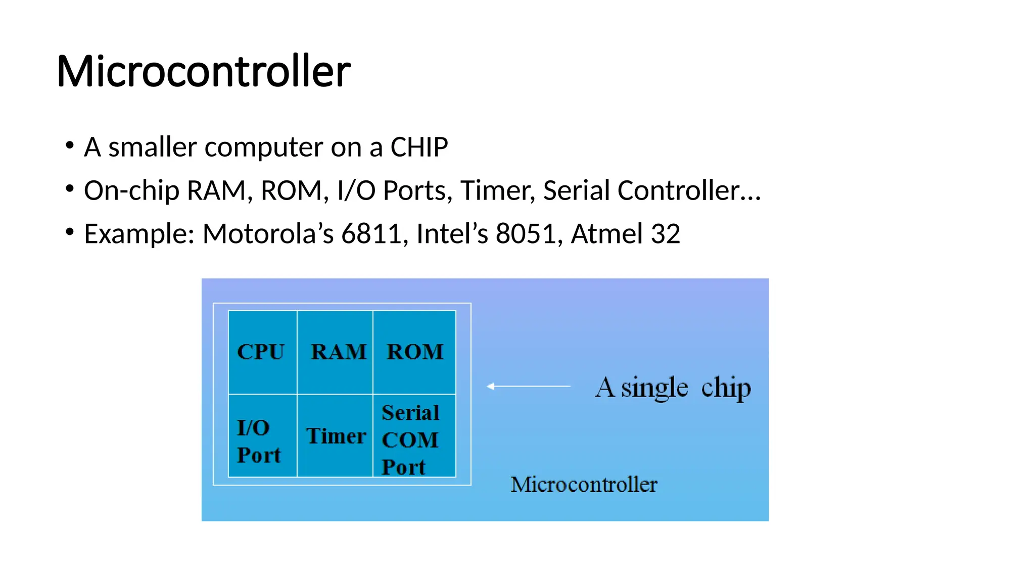
Microcontroller • A smallercomputer on a CHIP • On-chip RAM, ROM, I/O Ports, Timer, Serial Controller… • Example: Motorola’s 6811, Intel’s 8051, Atmel 32
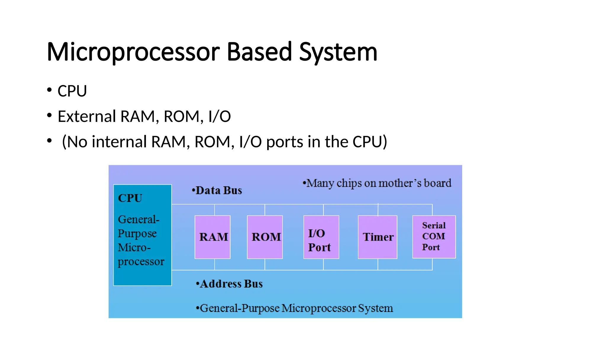
5.
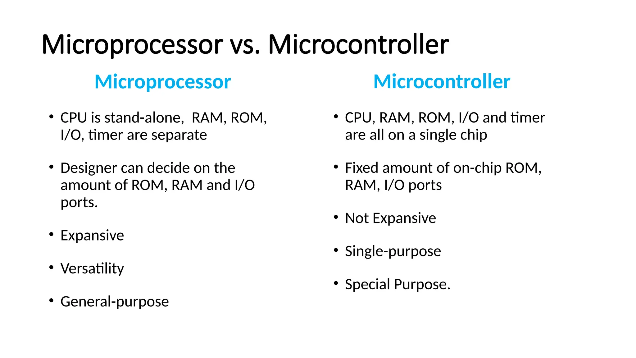
Microprocessor vs. Microcontroller Microprocessor •CPU is stand-alone, RAM, ROM, I/O, timer are separate • Designer can decide on the amount of ROM, RAM and I/O ports. • Expansive • Versatility • General-purpose Microcontroller • CPU, RAM, ROM, I/O and timer are all on a single chip • Fixed amount of on-chip ROM, RAM, I/O ports • Not Expansive • Single-purpose • Special Purpose.
6.
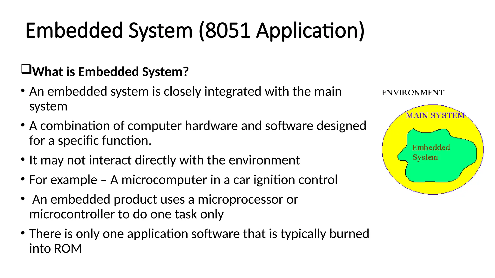
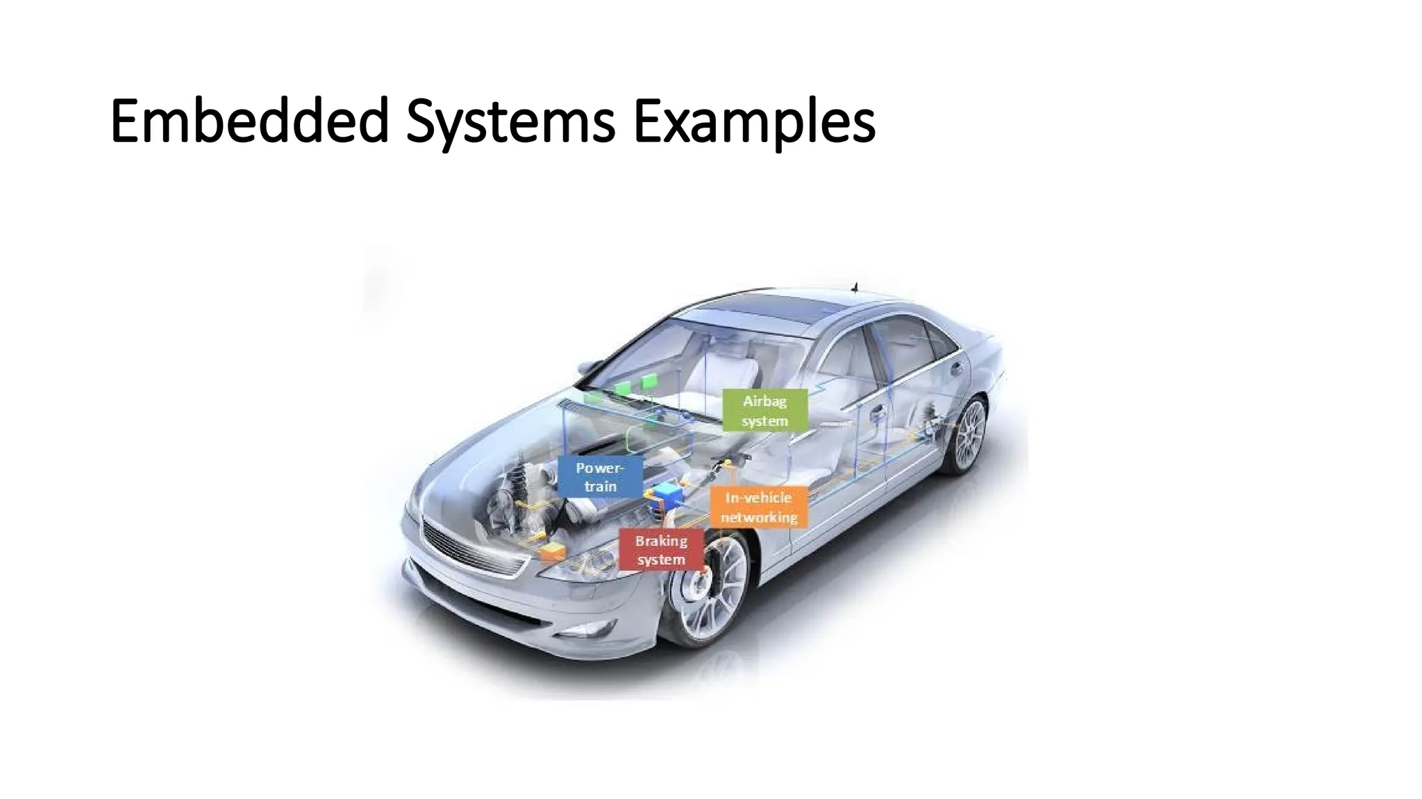
Embedded System (8051Application) What is Embedded System? • An embedded system is closely integrated with the main system • A combination of computer hardware and software designed for a specific function. • It may not interact directly with the environment • For example – A microcomputer in a car ignition control • An embedded product uses a microprocessor or microcontroller to do one task only • There is only one application software that is typically burned into ROM
C based EmbeddedSystems • Special purpose computer system usually completely inside the device it controls. • Has specific requirements and performs pre-defined tasks • PC contains or is connected to various embedded products • –Keyboard, printer, modem, disk controller, sound card, CD-ROM driver, mouse • Cost reduction compared to general purpose processor • Different design criteria • Performance • Reliability • Availability • Safety
9.
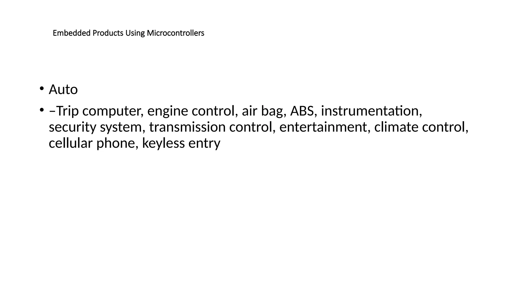
Embedded Products UsingMicrocontrollers • Home • –Appliances, intercom, telephones, security systems, garage door openers, answering machines, fax machines, home computers, TVs, cable TV tuner, VCR, camcorder, remote controls, video games, cellular phones, musical instruments, sewing machines, lighting control, paging, camera, pinball machines, toys, exercise equipment
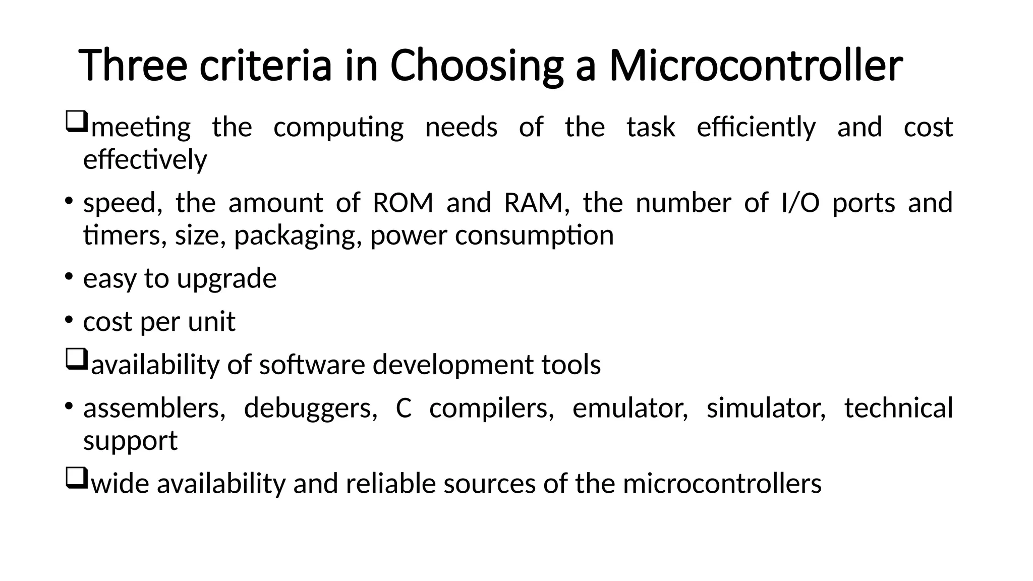
Three criteria inChoosing a Microcontroller meeting the computing needs of the task efficiently and cost effectively • speed, the amount of ROM and RAM, the number of I/O ports and timers, size, packaging, power consumption • easy to upgrade • cost per unit availability of software development tools • assemblers, debuggers, C compilers, emulator, simulator, technical support wide availability and reliable sources of the microcontrollers
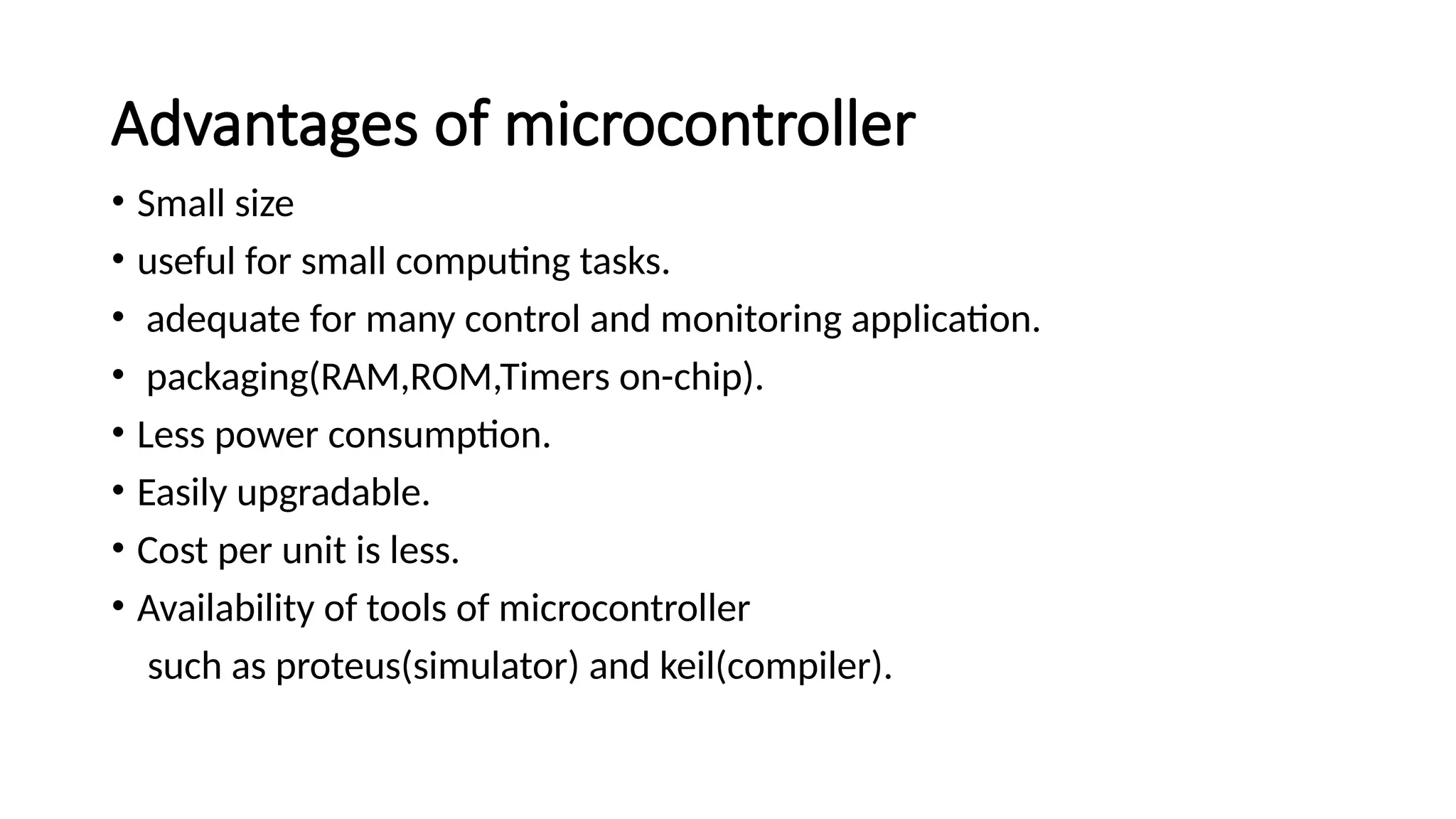
Advantages of microcontroller •Small size • useful for small computing tasks. • adequate for many control and monitoring application. • packaging(RAM,ROM,Timers on-chip). • Less power consumption. • Easily upgradable. • Cost per unit is less. • Availability of tools of microcontroller such as proteus(simulator) and keil(compiler).
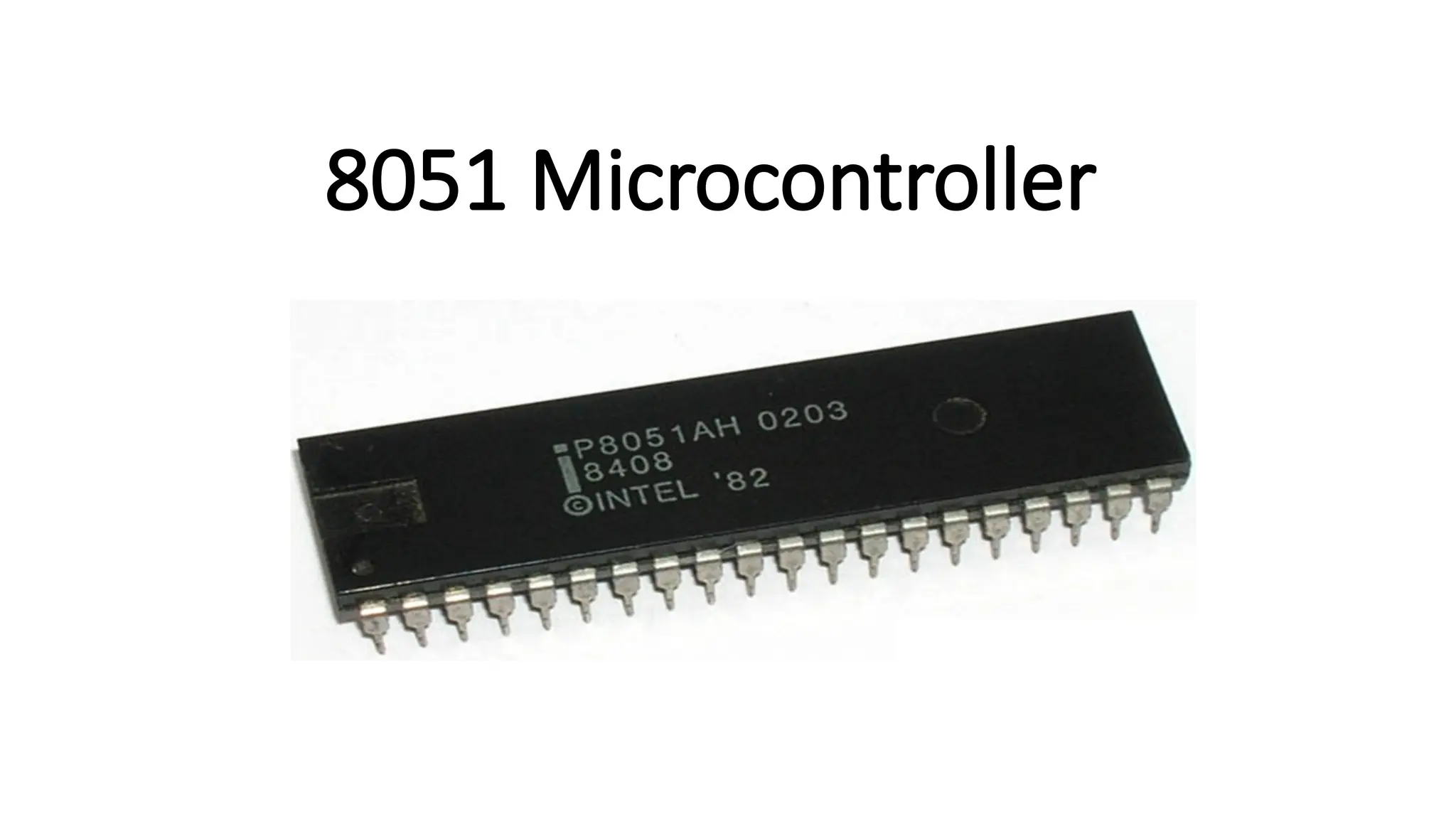
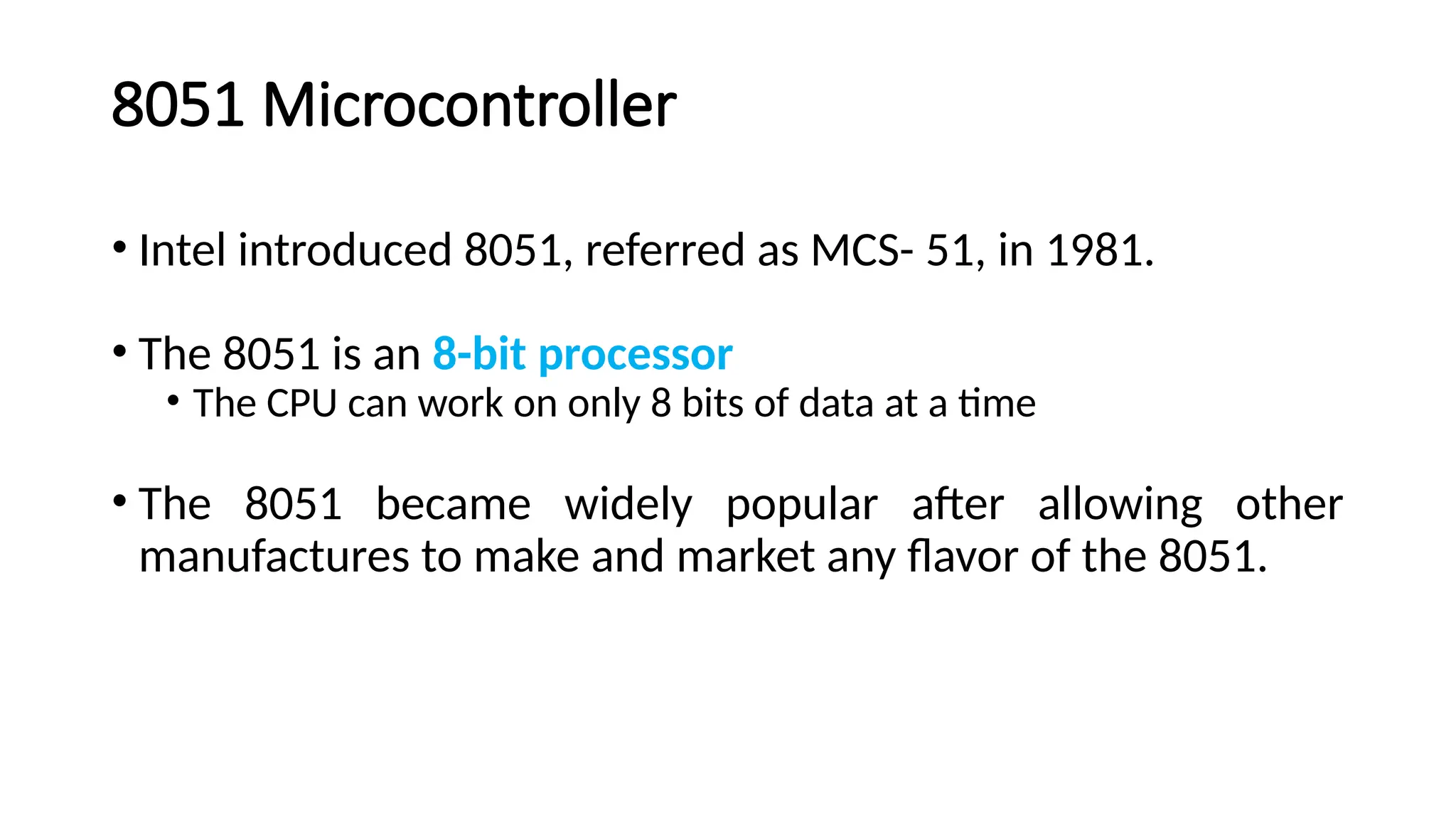
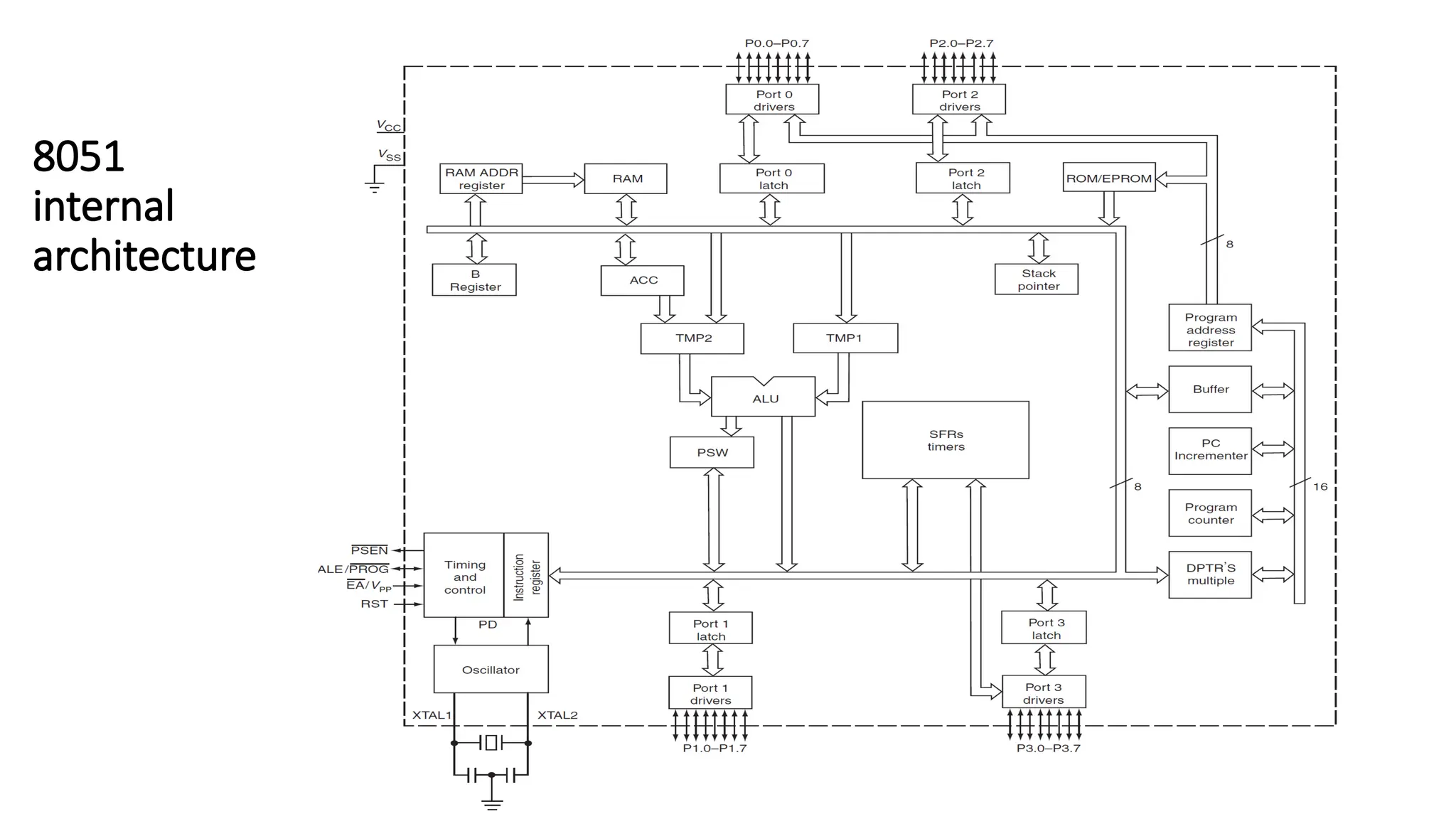
8051 Microcontroller • Intelintroduced 8051, referred as MCS- 51, in 1981. • The 8051 is an 8-bit processor • The CPU can work on only 8 bits of data at a time • The 8051 became widely popular after allowing other manufactures to make and market any flavor of the 8051.
18.
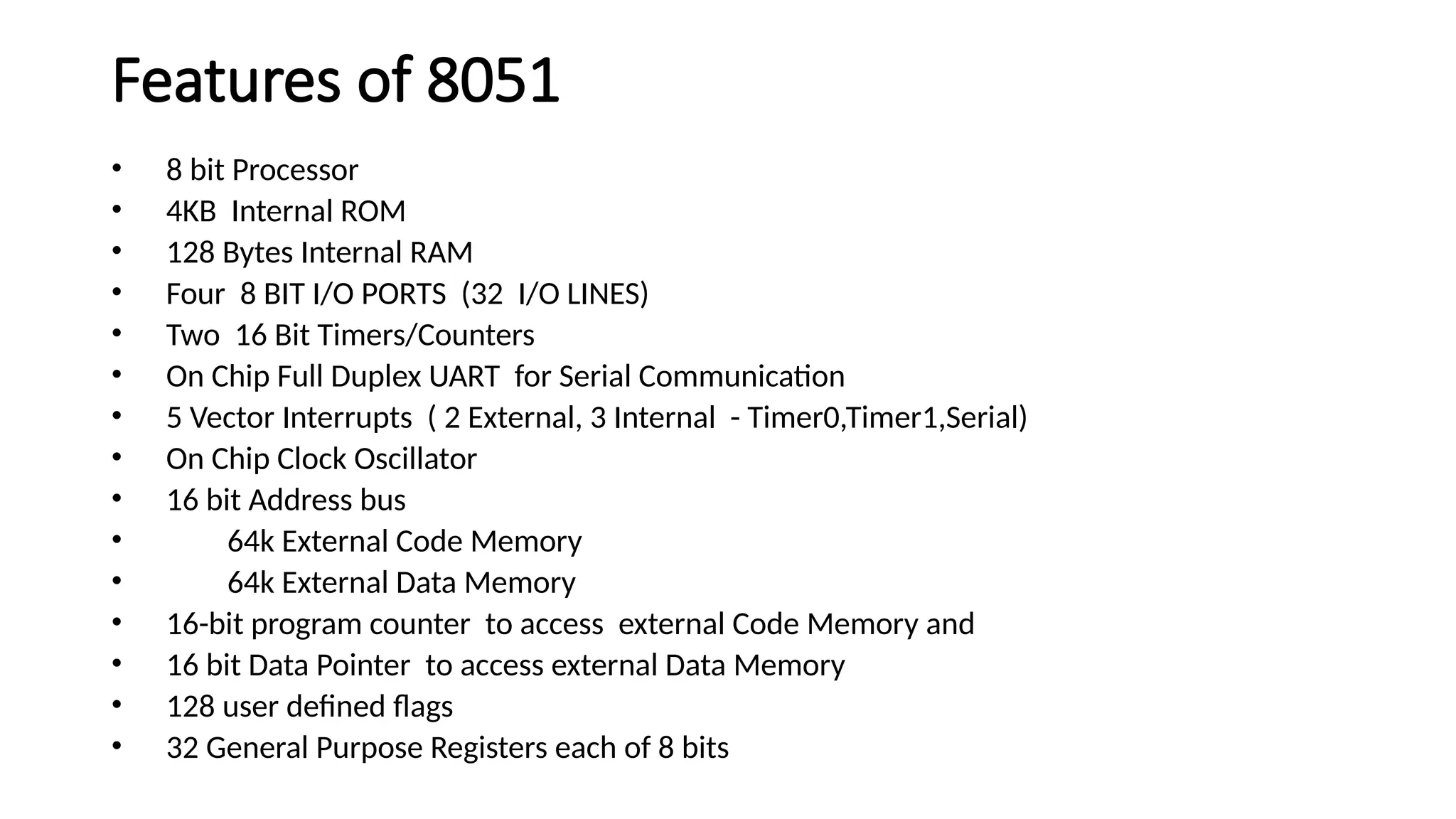
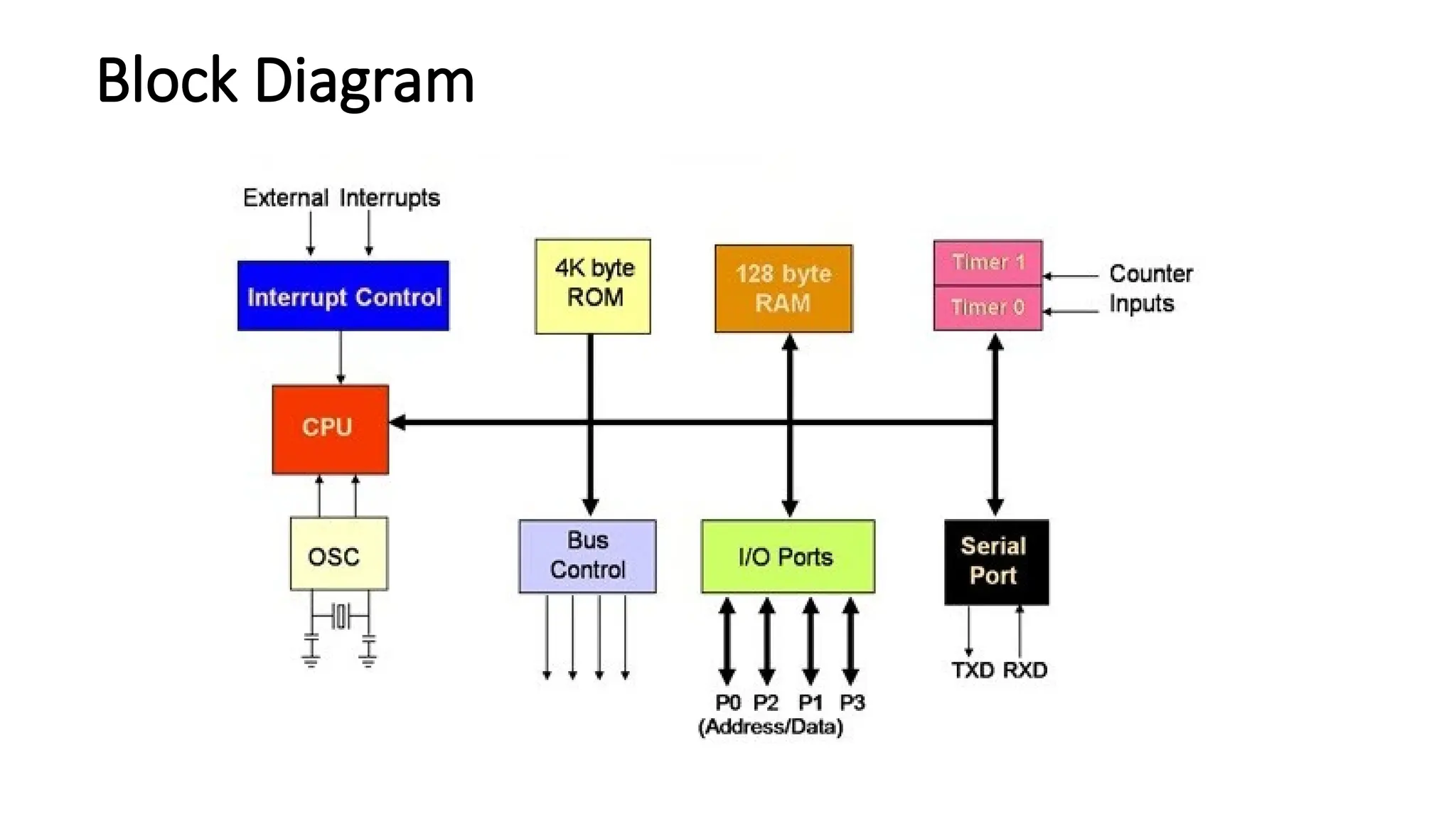
Features of 8051 •8 bit Processor • 4KB Internal ROM • 128 Bytes Internal RAM • Four 8 BIT I/O PORTS (32 I/O LINES) • Two 16 Bit Timers/Counters • On Chip Full Duplex UART for Serial Communication • 5 Vector Interrupts ( 2 External, 3 Internal - Timer0,Timer1,Serial) • On Chip Clock Oscillator • 16 bit Address bus • 64k External Code Memory • 64k External Data Memory • 16-bit program counter to access external Code Memory and • 16 bit Data Pointer to access external Data Memory • 128 user defined flags • 32 General Purpose Registers each of 8 bits
19.
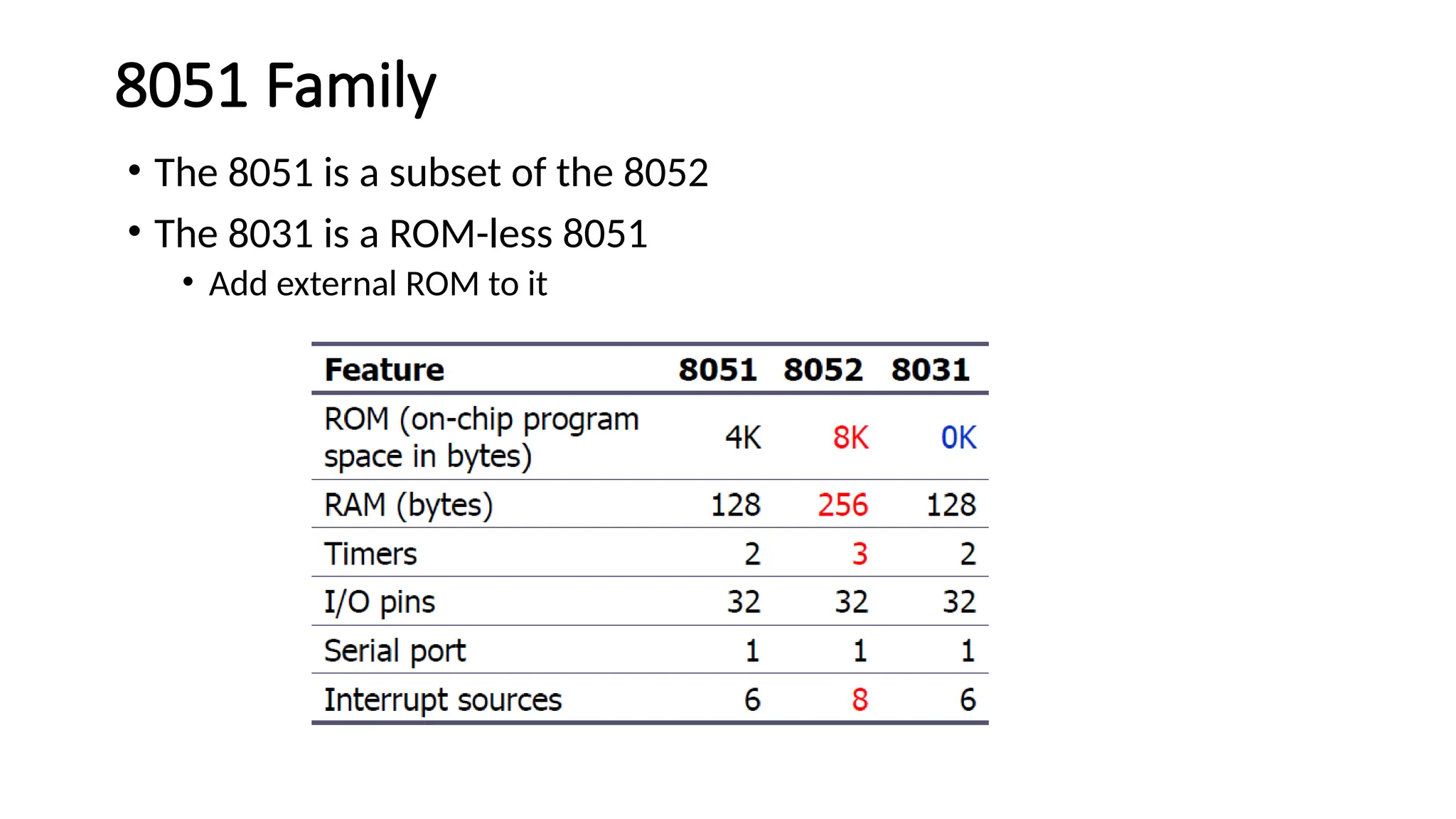
8051 Family • The8051 is a subset of the 8052 • The 8031 is a ROM-less 8051 • Add external ROM to it
20.
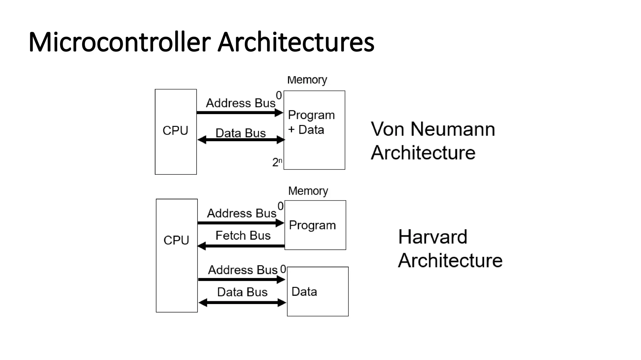
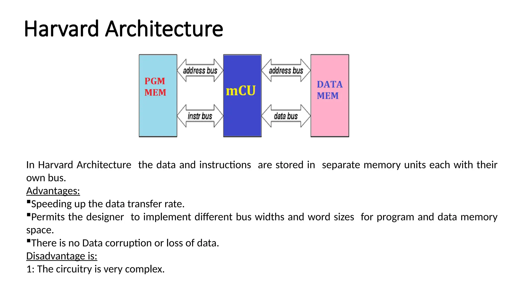
Harvard Architecture In HarvardArchitecture the data and instructions are stored in separate memory units each with their own bus. Advantages: Speeding up the data transfer rate. Permits the designer to implement different bus widths and word sizes for program and data memory space. There is no Data corruption or loss of data. Disadvantage is: 1: The circuitry is very complex.
21.
The necessary toolsfor a microcontroller • CPU: Central Processing Unit • I/O: Input /Output • Bus: Address bus & Data bus • Memory: RAM & ROM • Timer • Interrupt • Serial Port
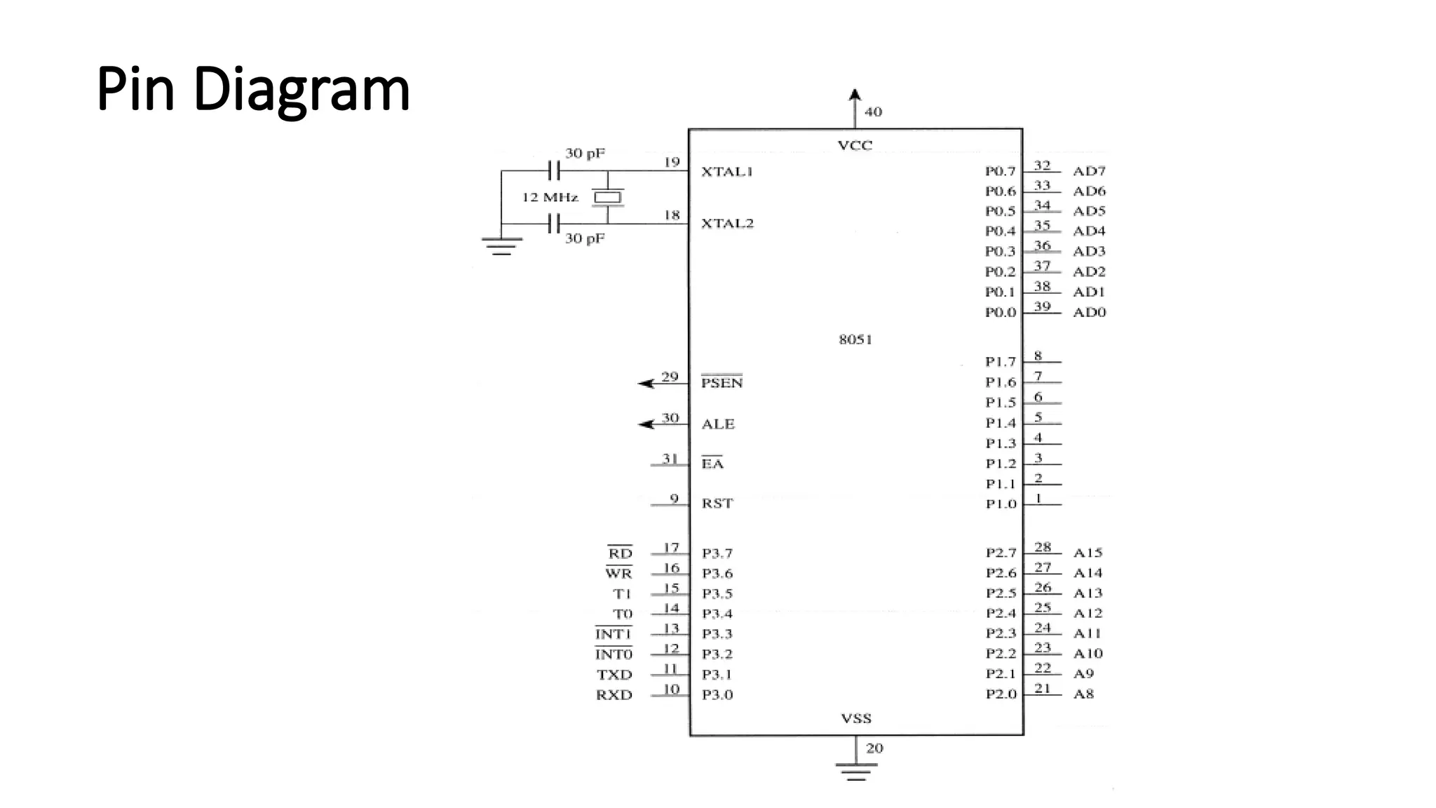
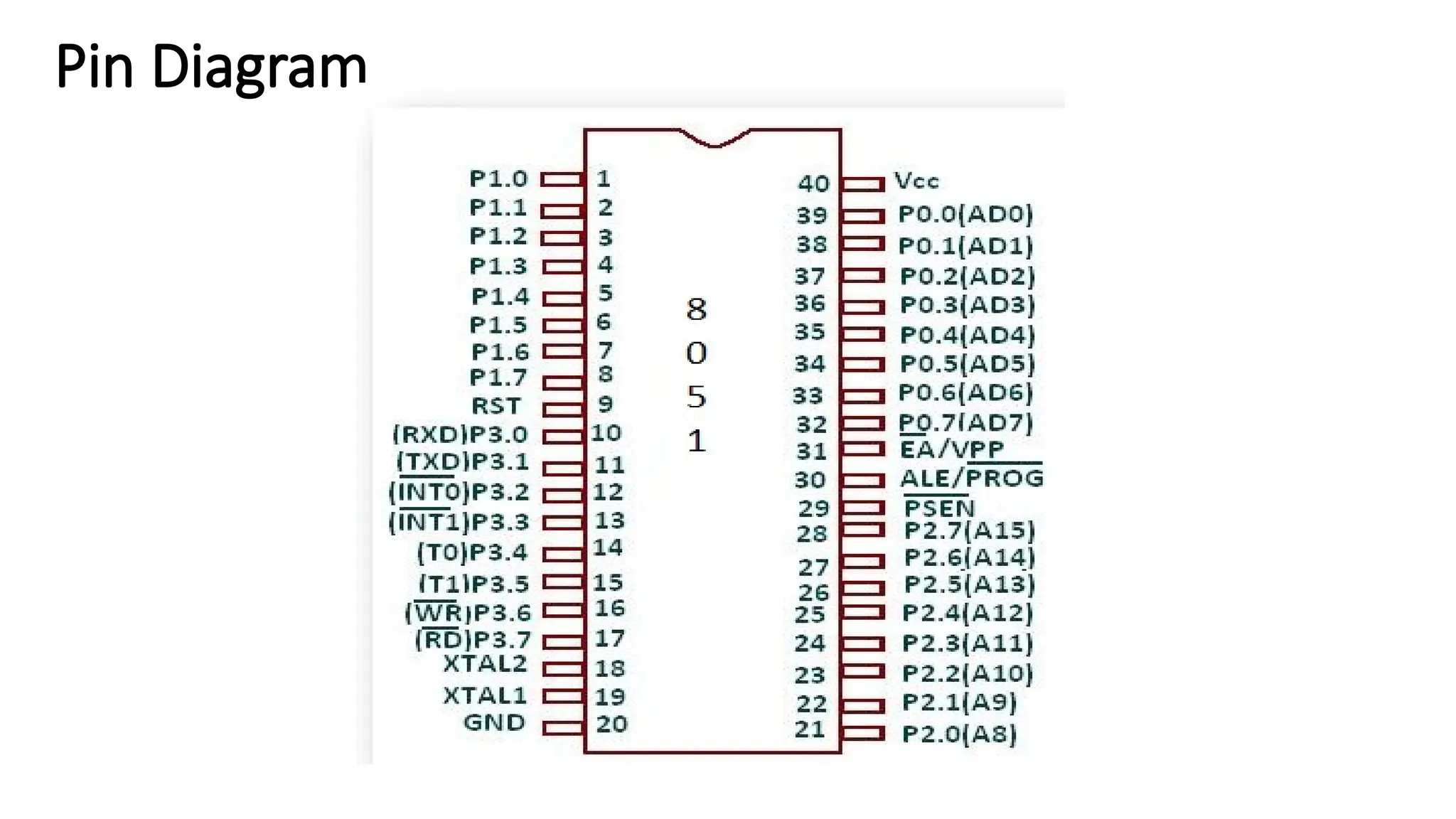
Pin Description ofthe 8051 • 8051 have 40 pins dedicated for various functions such as I/O, RD, WR, address, data, and interrupts. • Come in different packages, such as • DIP(dual in-line package), • QFP(quad flat package), and • LLC(leadless chip carrier) • Some companies provide a 20-pin version of the 8051 with a reduced number of I/O ports for less demanding applications.
26.
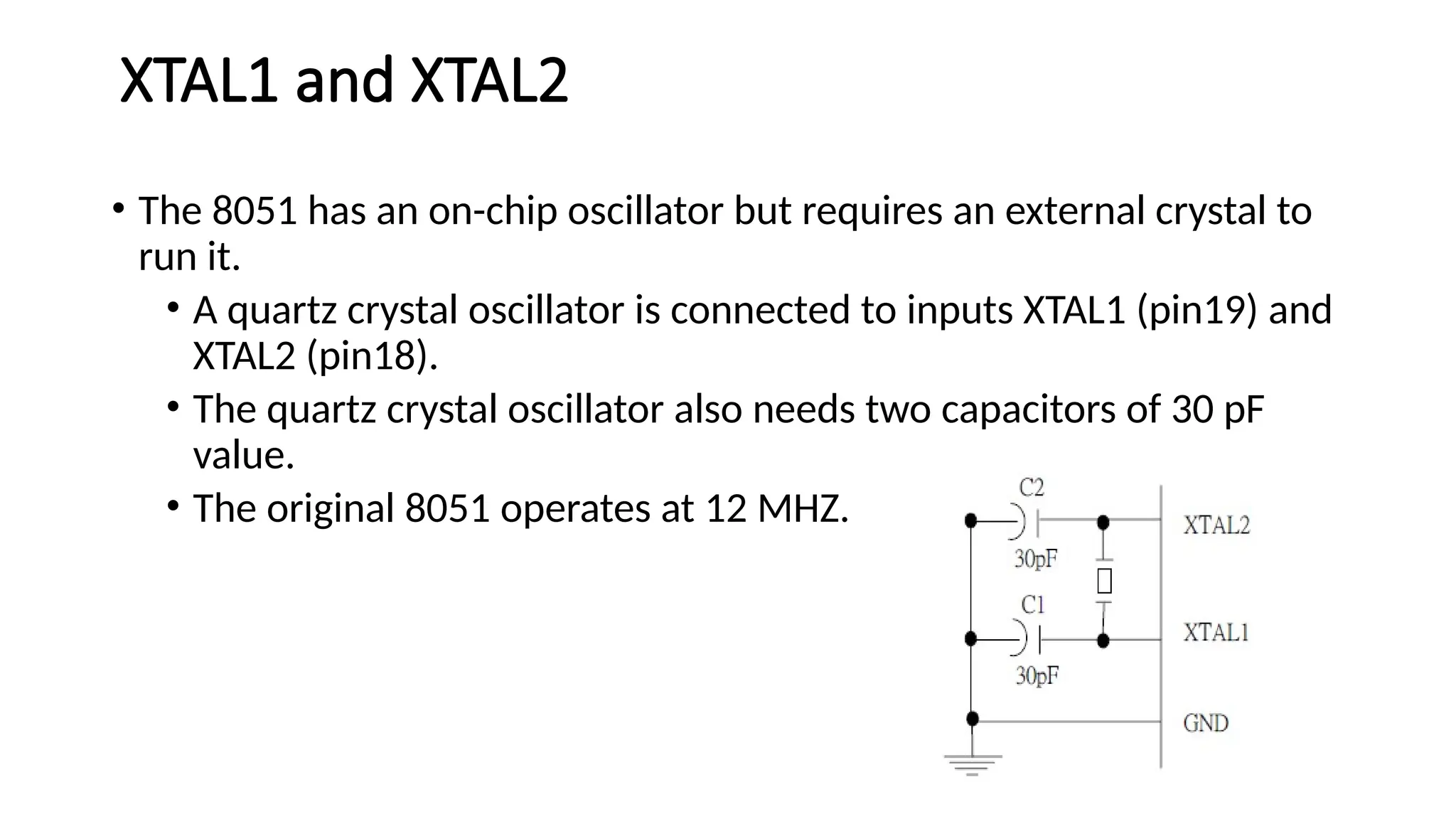
XTAL1 and XTAL2 •The 8051 has an on-chip oscillator but requires an external crystal to run it. • A quartz crystal oscillator is connected to inputs XTAL1 (pin19) and XTAL2 (pin18). • The quartz crystal oscillator also needs two capacitors of 30 pF value. • The original 8051 operates at 12 MHZ.
27.
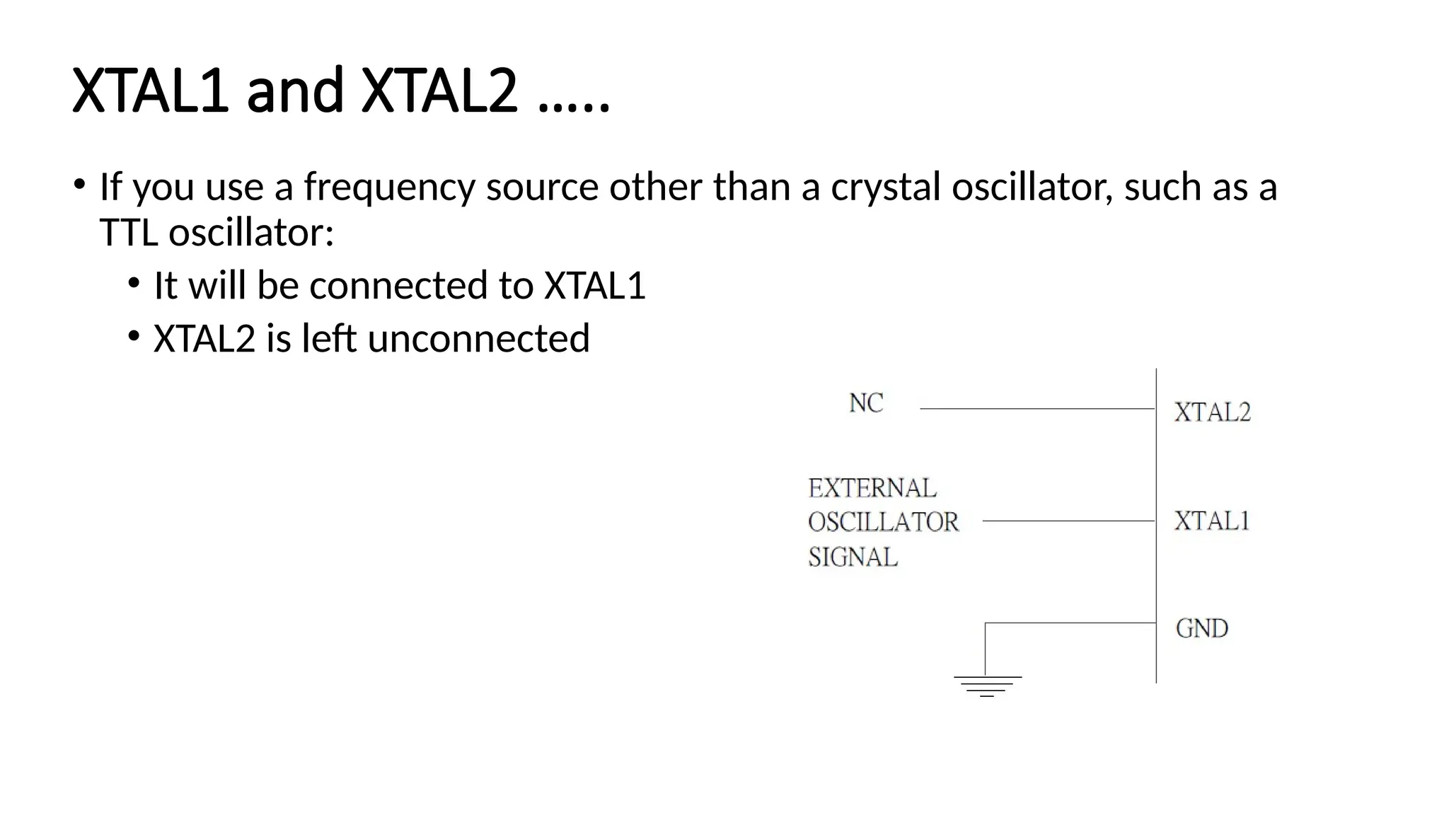
XTAL1 and XTAL2….. • If you use a frequency source other than a crystal oscillator, such as a TTL oscillator: • It will be connected to XTAL1 • XTAL2 is left unconnected
28.
RST • RESET pinis an input and is active high (normally low during the 8051 operation). • Upon applying a high pulse to this pin, the microcontroller will reset and terminate all activities. • This is often referred to as a power-on reset. • Activating a power-on reset will cause all values in the registers to be lost.
29.
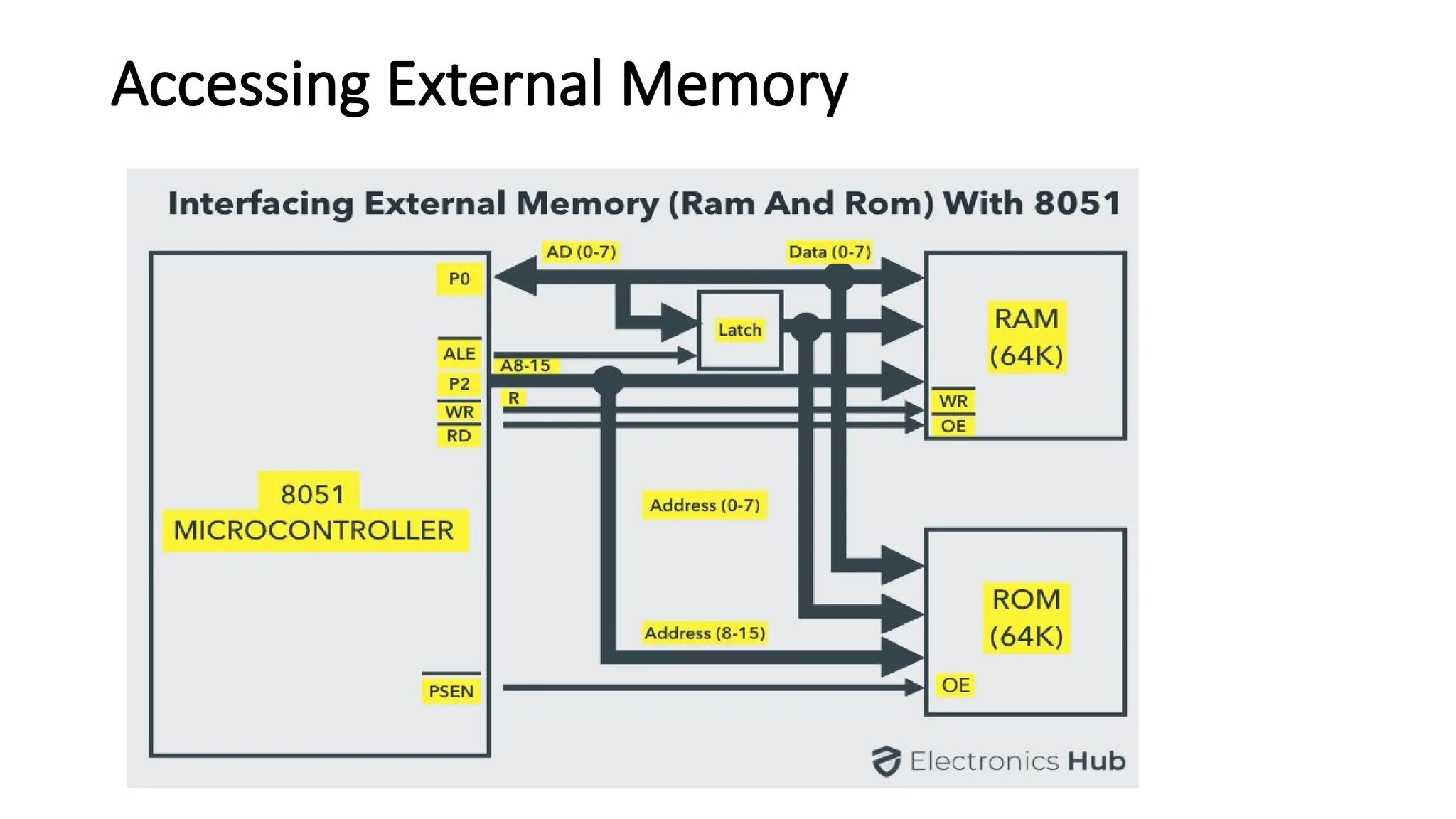
EA • EA, “externalaccess’’, is an input pin and must be connected to Vcc or GND • The 8051 family members all come with on-chip ROM to store programs and also have an external code and data memory. • Normally EA pin is connected to Vcc (Internal Access) • EA pin must be connected to GND to indicate that the code or data is stored externally.
30.
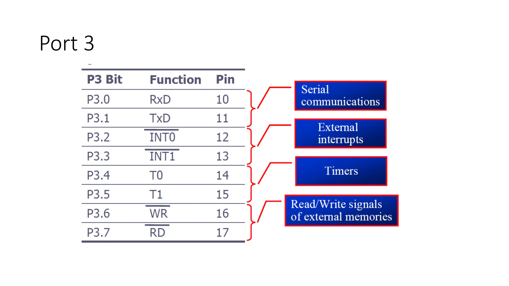
PSEN and ALE •PSEN, “program store enable’’, is an output pin • This pin is connected to the OE pin of the external memory. • For External Code Memory, PSEN = 0 • For External Data Memory, PSEN = 1 • ALE pin is used for demultiplexing the address and data.
31.
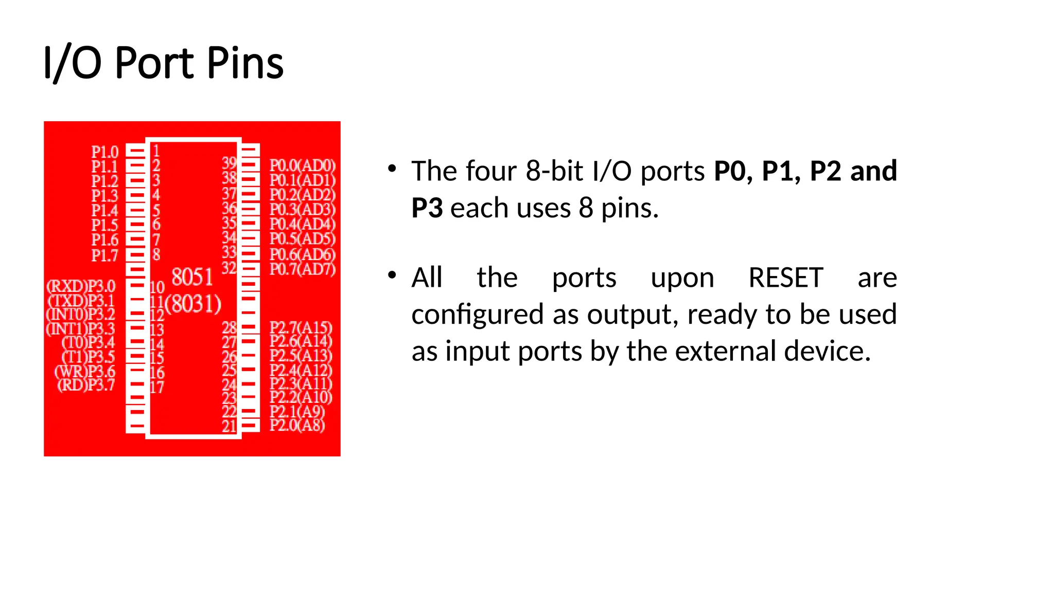
I/O Port Pins •The four 8-bit I/O ports P0, P1, P2 and P3 each uses 8 pins. • All the ports upon RESET are configured as output, ready to be used as input ports by the external device.
32.
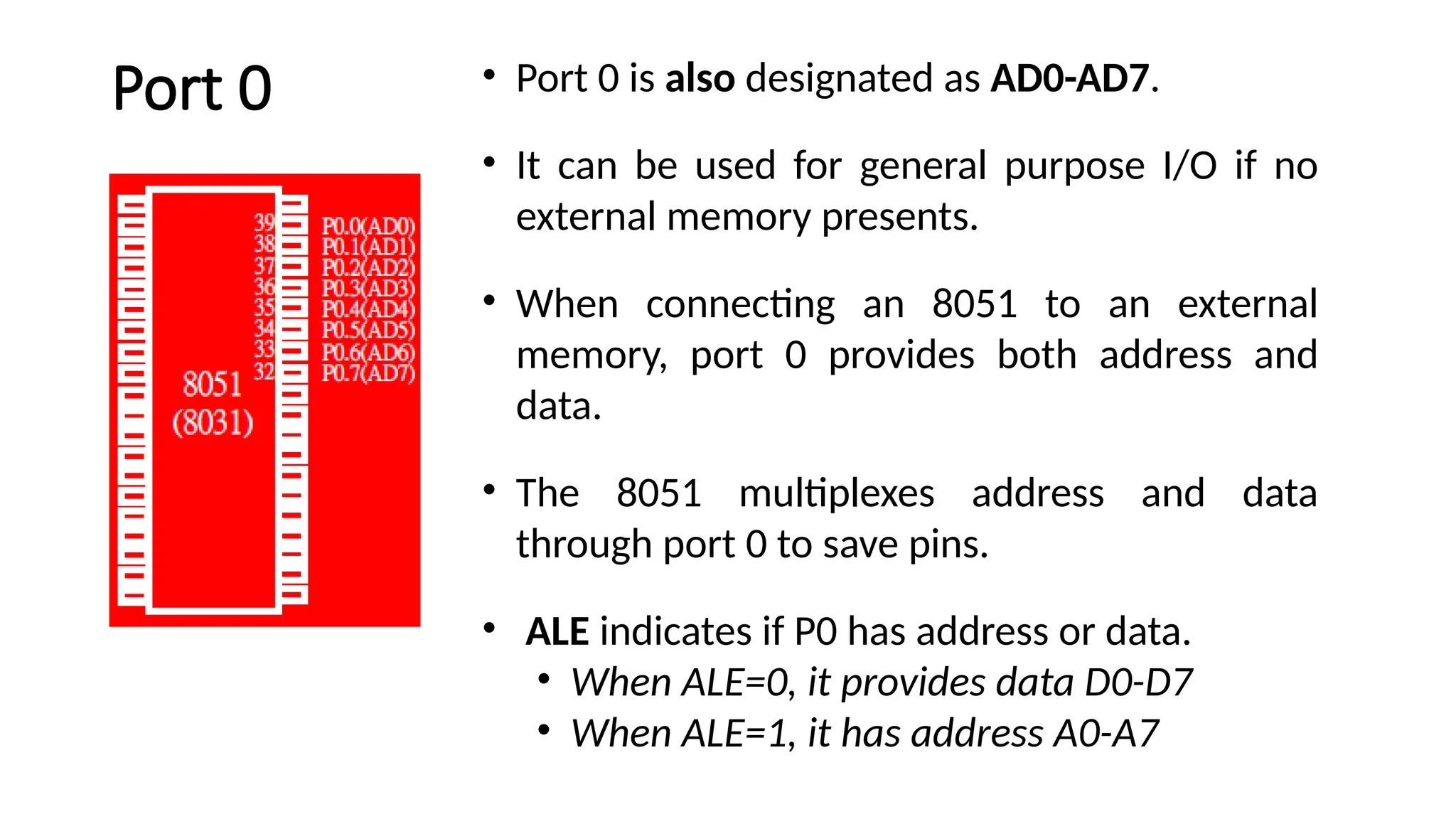
Port 0 •Port 0 is also designated as AD0-AD7. • It can be used for general purpose I/O if no external memory presents. • When connecting an 8051 to an external memory, port 0 provides both address and data. • The 8051 multiplexes address and data through port 0 to save pins. • ALE indicates if P0 has address or data. • When ALE=0, it provides data D0-D7 • When ALE=1, it has address A0-A7
33.
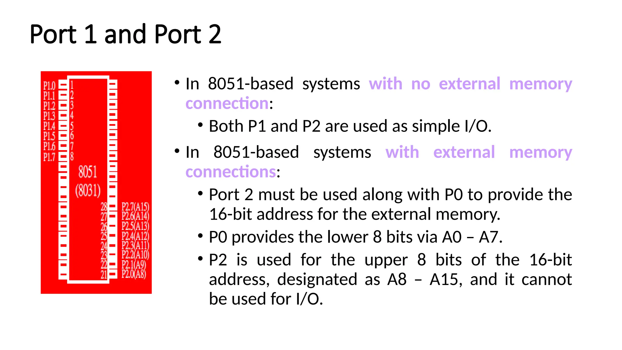
Port 1 andPort 2 • In 8051-based systems with no external memory connection: • Both P1 and P2 are used as simple I/O. • In 8051-based systems with external memory connections: • Port 2 must be used along with P0 to provide the 16-bit address for the external memory. • P0 provides the lower 8 bits via A0 – A7. • P2 is used for the upper 8 bits of the 16-bit address, designated as A8 – A15, and it cannot be used for I/O.
Arithmetic and LogicUnit • Performing computing functions • Accumulator is 8-bit register • Arithmetic and logical operations – one of the operands is in A register • Result is stored in only A • C(carry), AC(auxiliary carry), O(overflow) and P(Parity) – status register
37.
Instruction decoder andcontrol • When an instruction is fetched – it is loaded in the instruction register • Decoder decodes the instruction and establishes the sequence of events to follow • Instruction cycle: Instruction cycle is defined as the time required for completing the execution of an instruction • Instruction register is not programmable • It cannot be accessed through any instruction • Control unit generates control signals necessary for communication between the processor and peripherals
38.
CPU A andB Registers A Register • 8 bit • Direct connection with ALU • A(accumulator) is used for addition,subtraction,mul,div,boolean bit manipulation and for data transfers. • In multiplication- one of 8 bit operands stored in A and after operation it stores lower byte in A • In division- holds 8 bit dividend & quotient is stored in A B Register • –8 bit • –Used with multiply and divide operations • –In multiplication- after operation it stores higher byte in B • –In division- holds 8 bit divisor & reminder is stored in B
39.
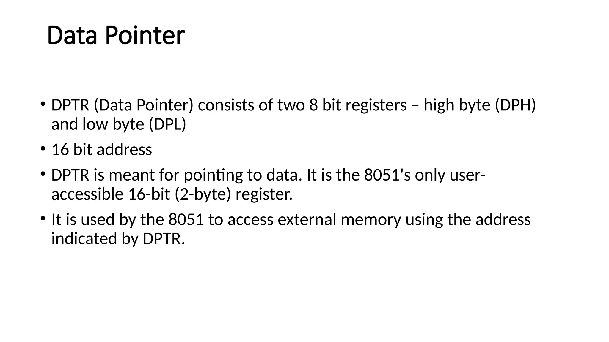
Data Pointer • DPTR(Data Pointer) consists of two 8 bit registers – high byte (DPH) and low byte (DPL) • 16 bit address • DPTR is meant for pointing to data. It is the 8051's only user- accessible 16-bit (2-byte) register. • It is used by the 8051 to access external memory using the address indicated by DPTR.
40.
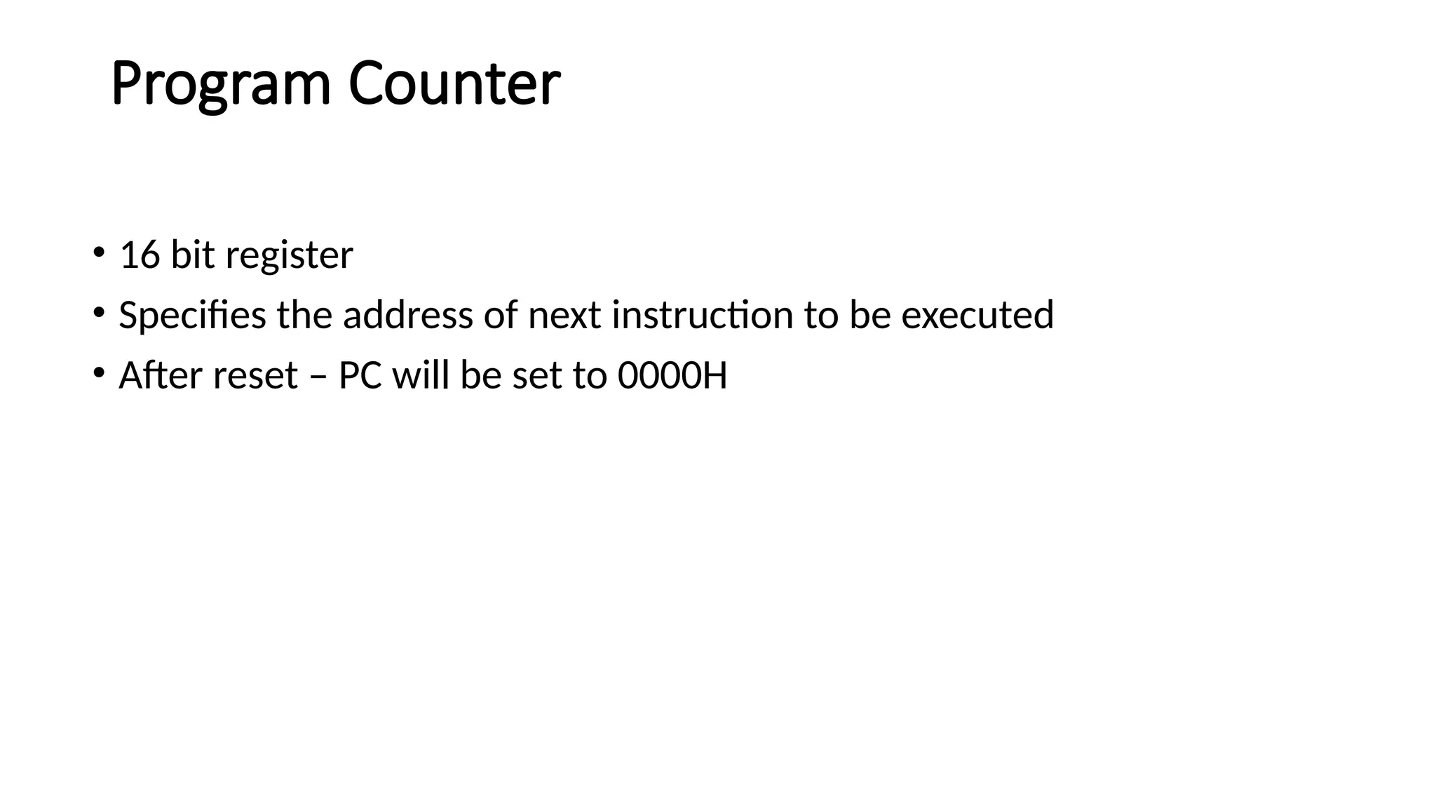
Program Counter • 16bit register • Specifies the address of next instruction to be executed • After reset – PC will be set to 0000H
41.
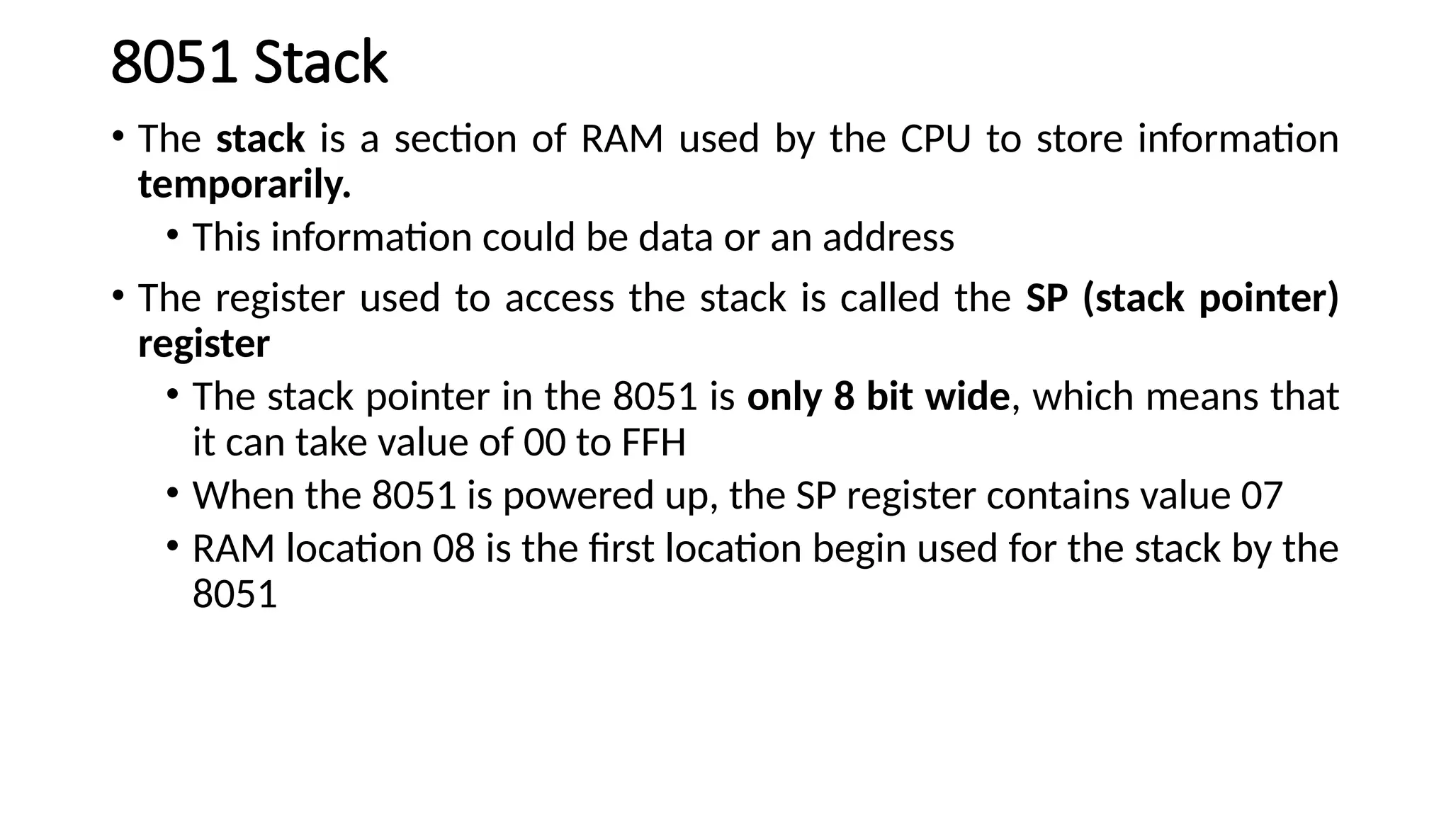
8051 Stack • Thestack is a section of RAM used by the CPU to store information temporarily. • This information could be data or an address • The register used to access the stack is called the SP (stack pointer) register • The stack pointer in the 8051 is only 8 bit wide, which means that it can take value of 00 to FFH • When the 8051 is powered up, the SP register contains value 07 • RAM location 08 is the first location begin used for the stack by the 8051
42.
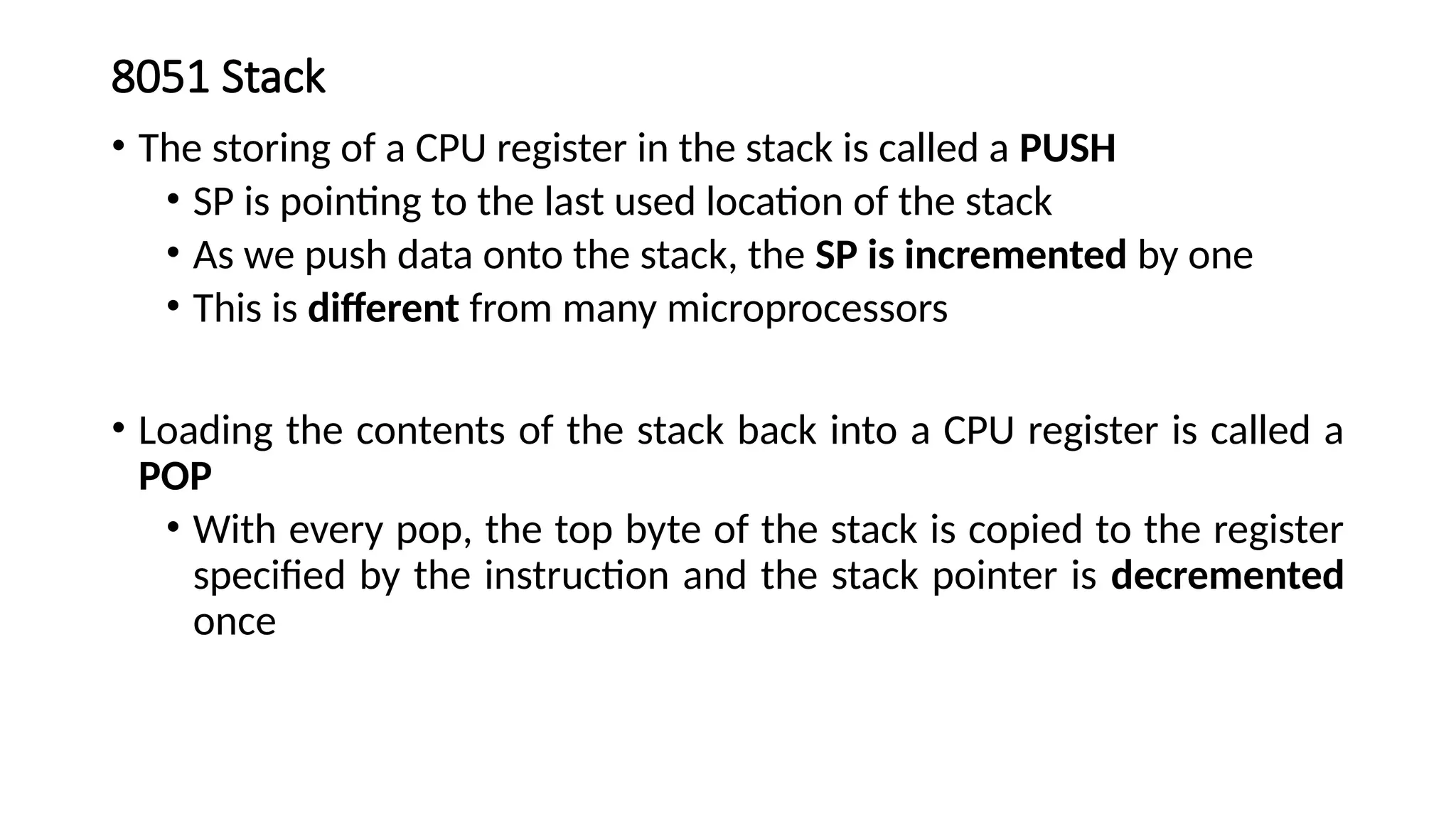
8051 Stack • Thestoring of a CPU register in the stack is called a PUSH • SP is pointing to the last used location of the stack • As we push data onto the stack, the SP is incremented by one • This is different from many microprocessors • Loading the contents of the stack back into a CPU register is called a POP • With every pop, the top byte of the stack is copied to the register specified by the instruction and the stack pointer is decremented once
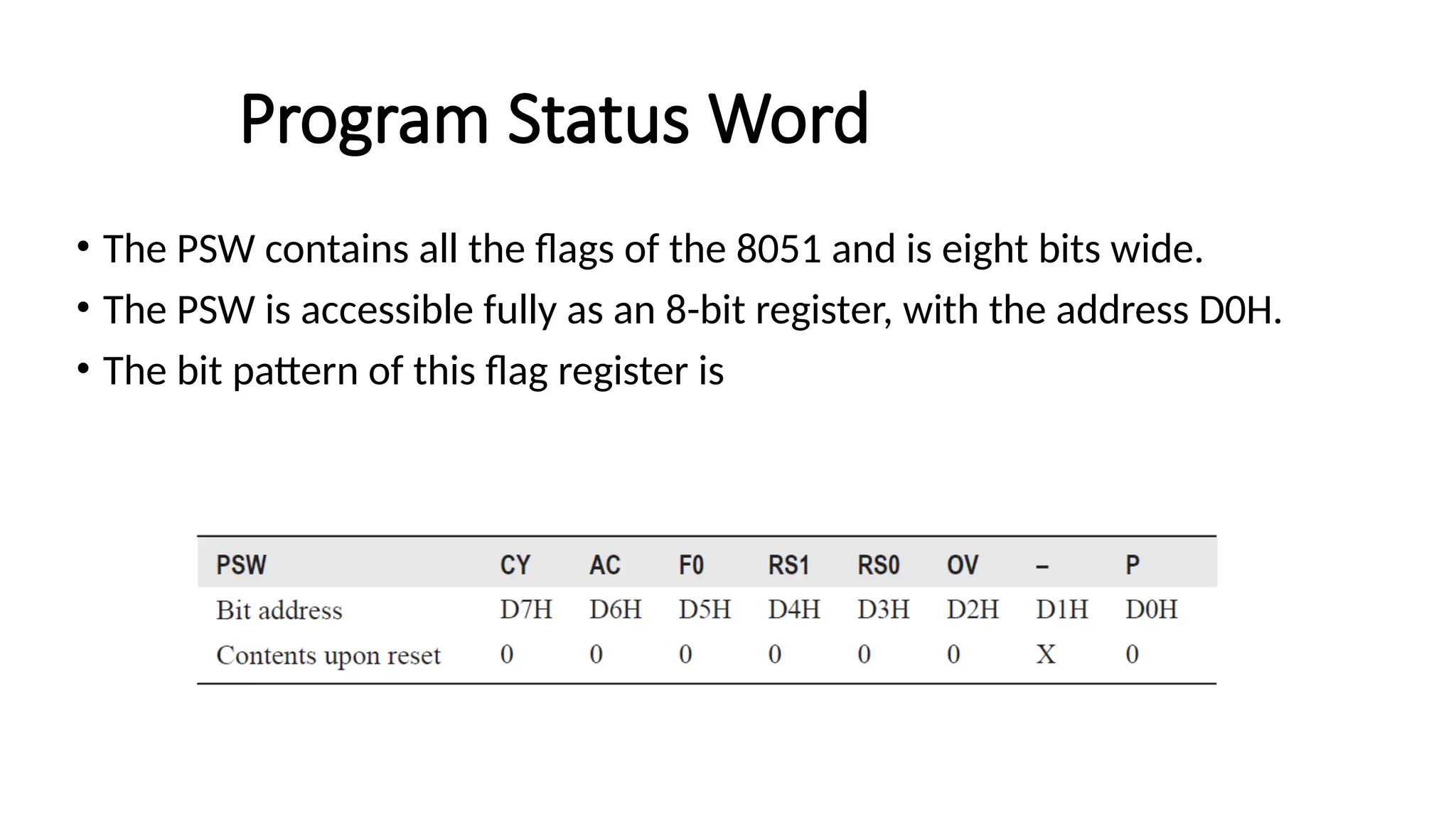
Program Status Word •The PSW contains all the flags of the 8051 and is eight bits wide. • The PSW is accessible fully as an 8-bit register, with the address D0H. • The bit pattern of this flag register is
45.
• Parity bit(P) • It is set to 1 if the accumulator contains an odd number of 1s, after an arithmetic or logical operation. • Overflow flag (OV) • This flag is set during ALU operations, to indicate overflow in the result. It is set to 1 if there is a carry out of either the D7 bit or the D6 bit of the accumulator. Overflow flag is set when arithmetic operations such as add and subtract result in sign conflict. • The conditions under which the OV flag is set are as follows: • Positive + Positive = Negative • Negative + Negative = Positive • Positive – Negative = Negative • Negative – Positive = Positive Flag Description
46.
Flag Description • Auxiliarycarry flag (AC) • It is used in association with BCD arithmetic. This flag is set when there is a carry out of the D3 bit of the accumulator. • Carry flag (CY) • This flag is used to indicate the carry generated after arithmetic operations.
47.
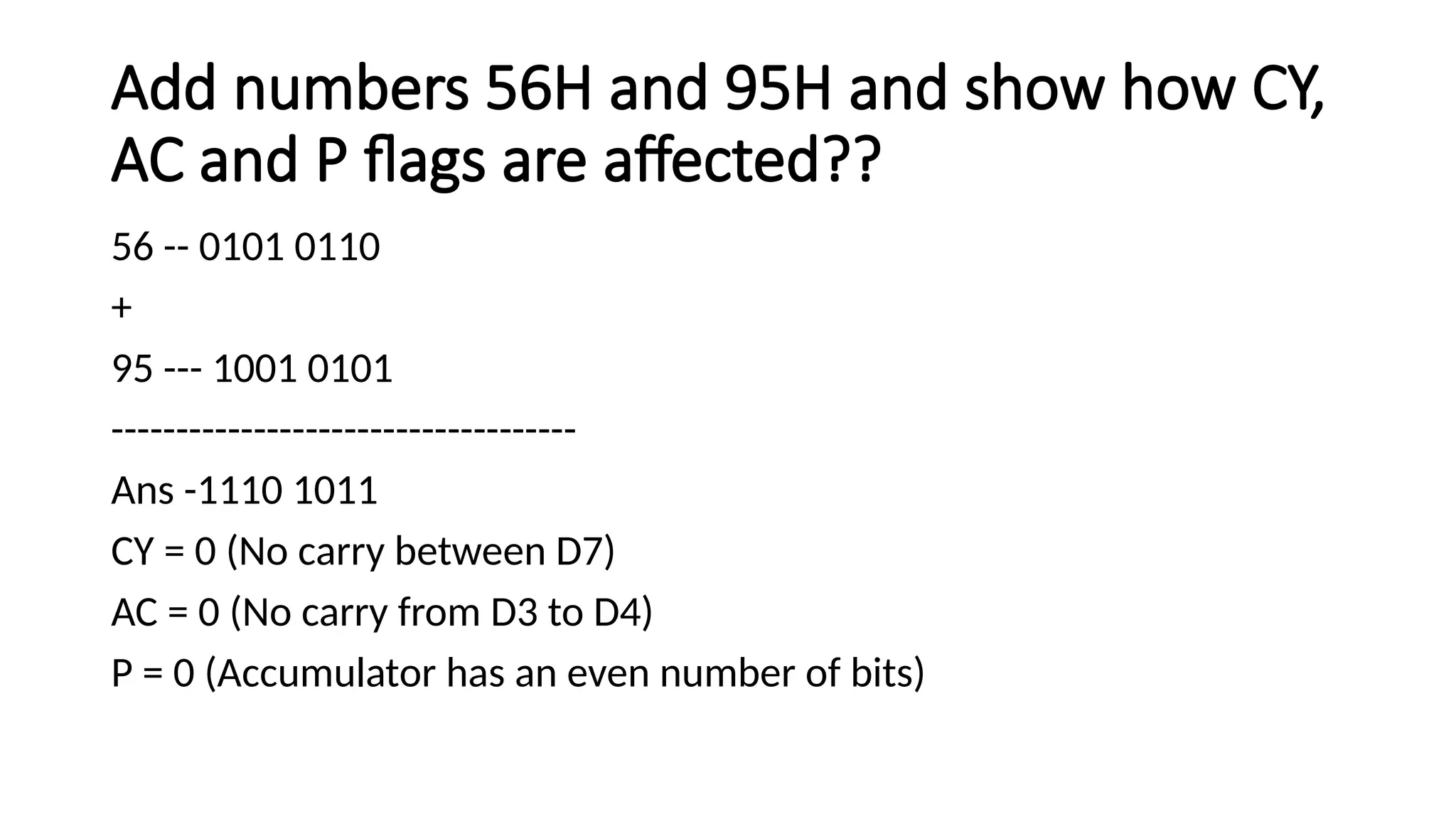
Add numbers 56Hand 95H and show how CY, AC and P flags are affected?? 56 -- 0101 0110 + 95 --- 1001 0101 ------------------------------------ Ans -1110 1011 CY = 0 (No carry between D7) AC = 0 (No carry from D3 to D4) P = 0 (Accumulator has an even number of bits)
48.
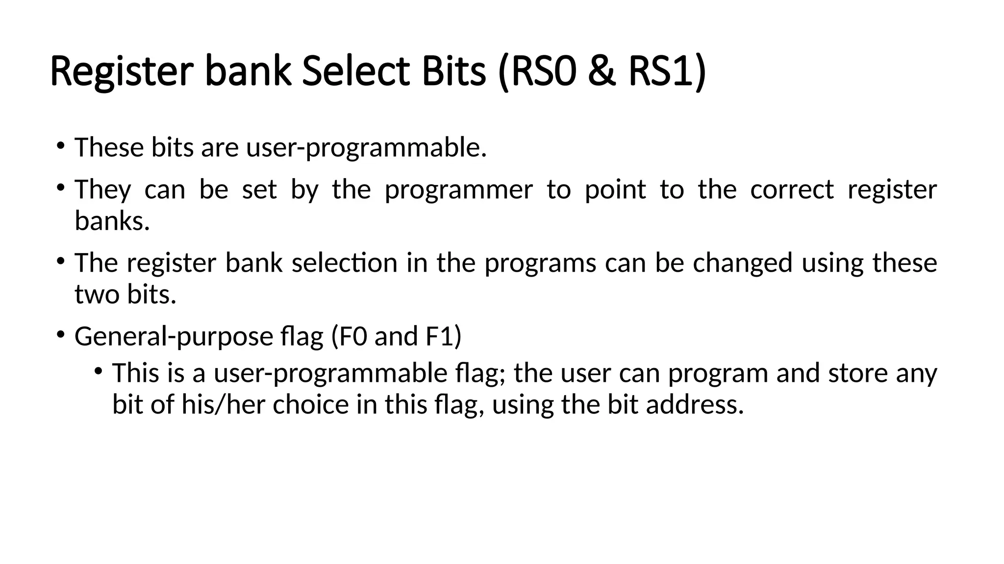
Register bank SelectBits (RS0 & RS1) • These bits are user-programmable. • They can be set by the programmer to point to the correct register banks. • The register bank selection in the programs can be changed using these two bits. • General-purpose flag (F0 and F1) • This is a user-programmable flag; the user can program and store any bit of his/her choice in this flag, using the bit address.
49.
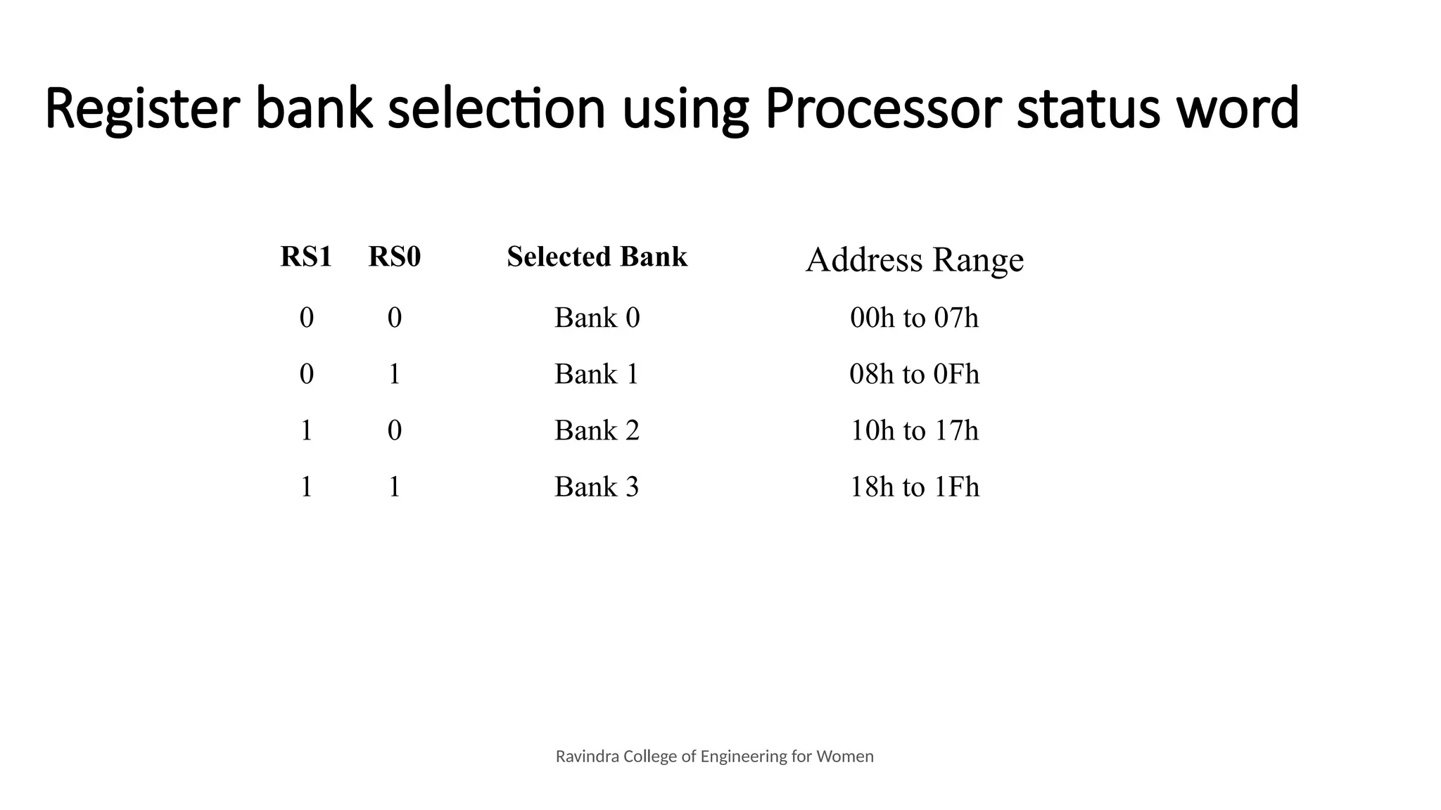
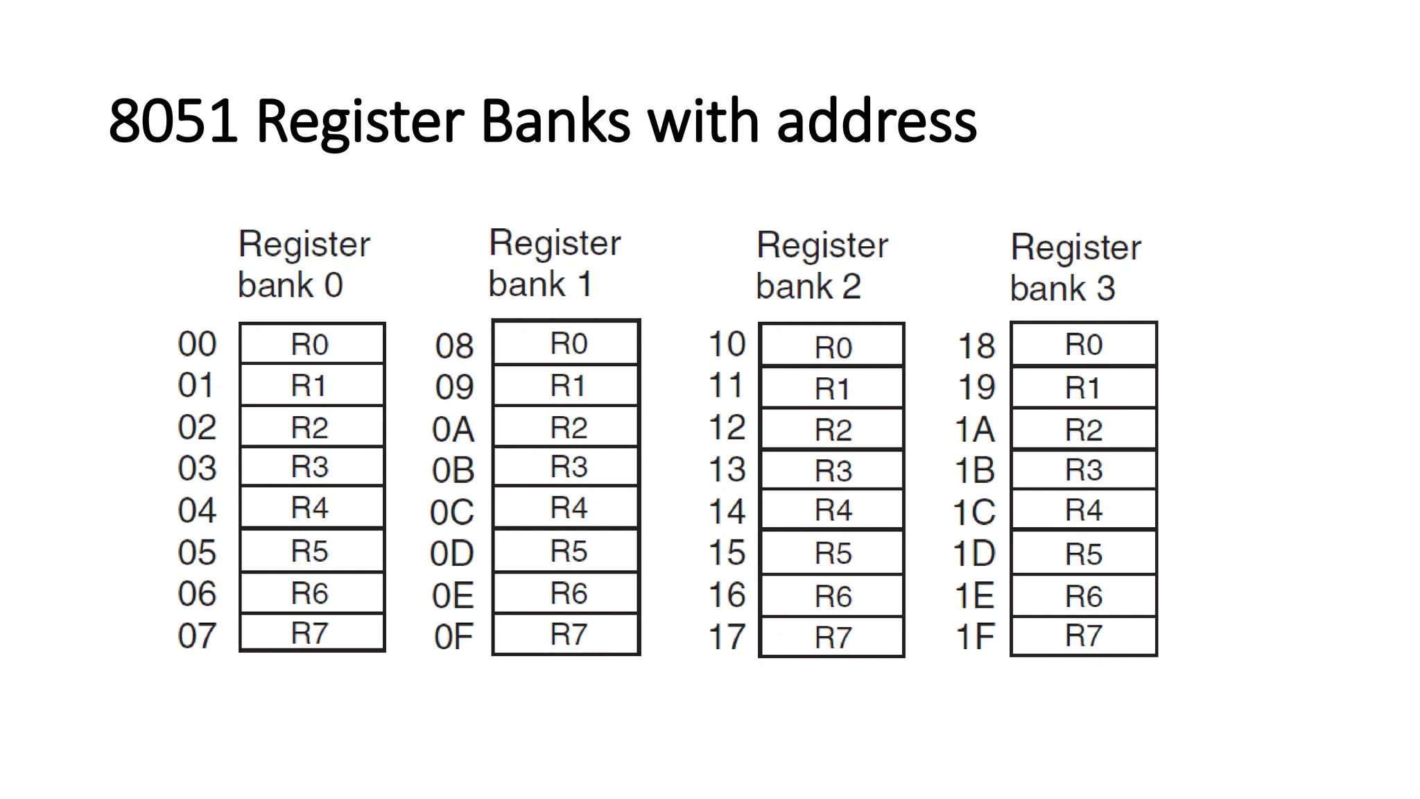
Register bank selectionusing Processor status word Ravindra College of Engineering for Women RS1 RS0 Selected Bank Address Range 0 0 Bank 0 00h to 07h 0 1 Bank 1 08h to 0Fh 1 0 Bank 2 10h to 17h 1 1 Bank 3 18h to 1Fh
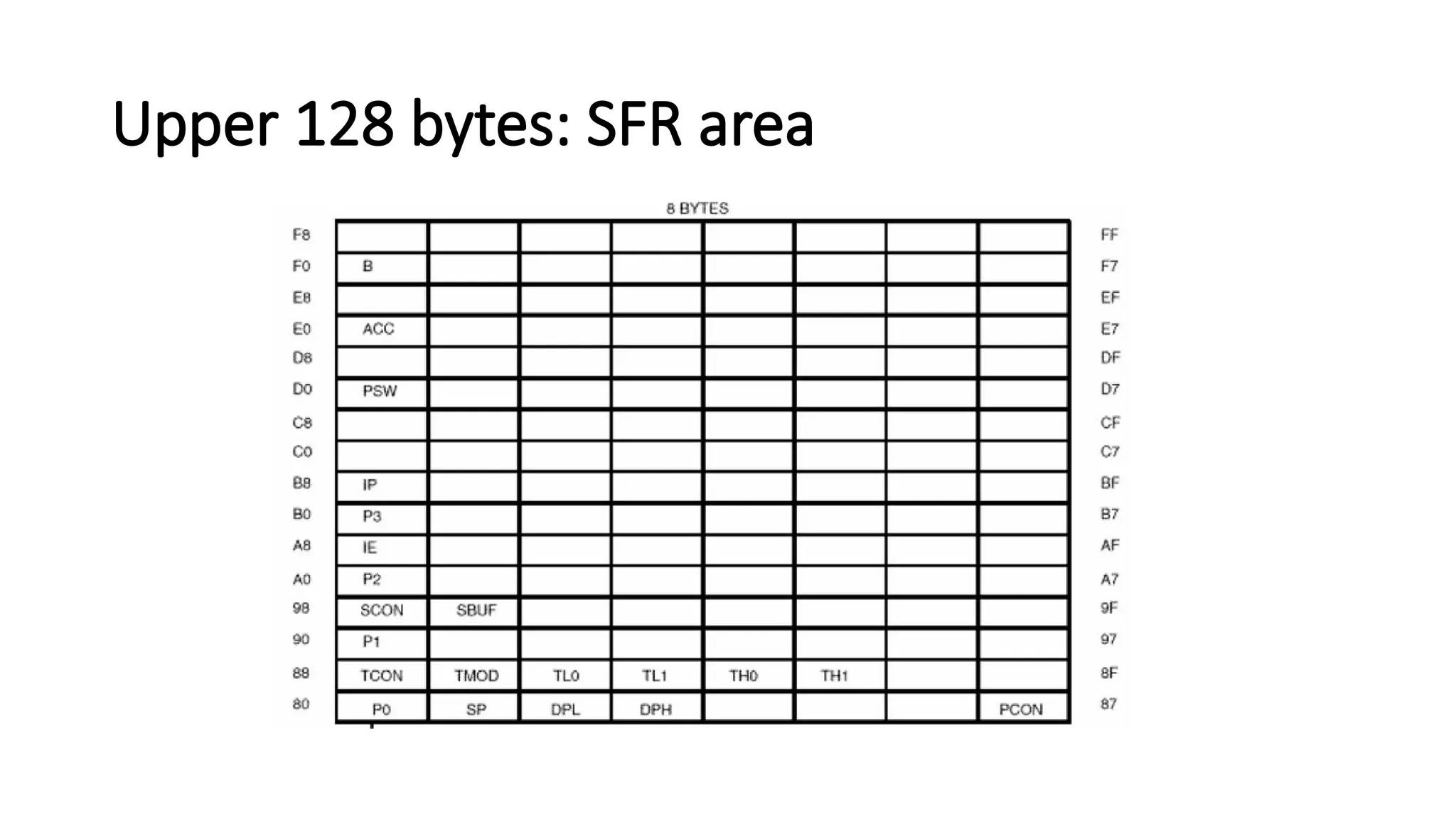
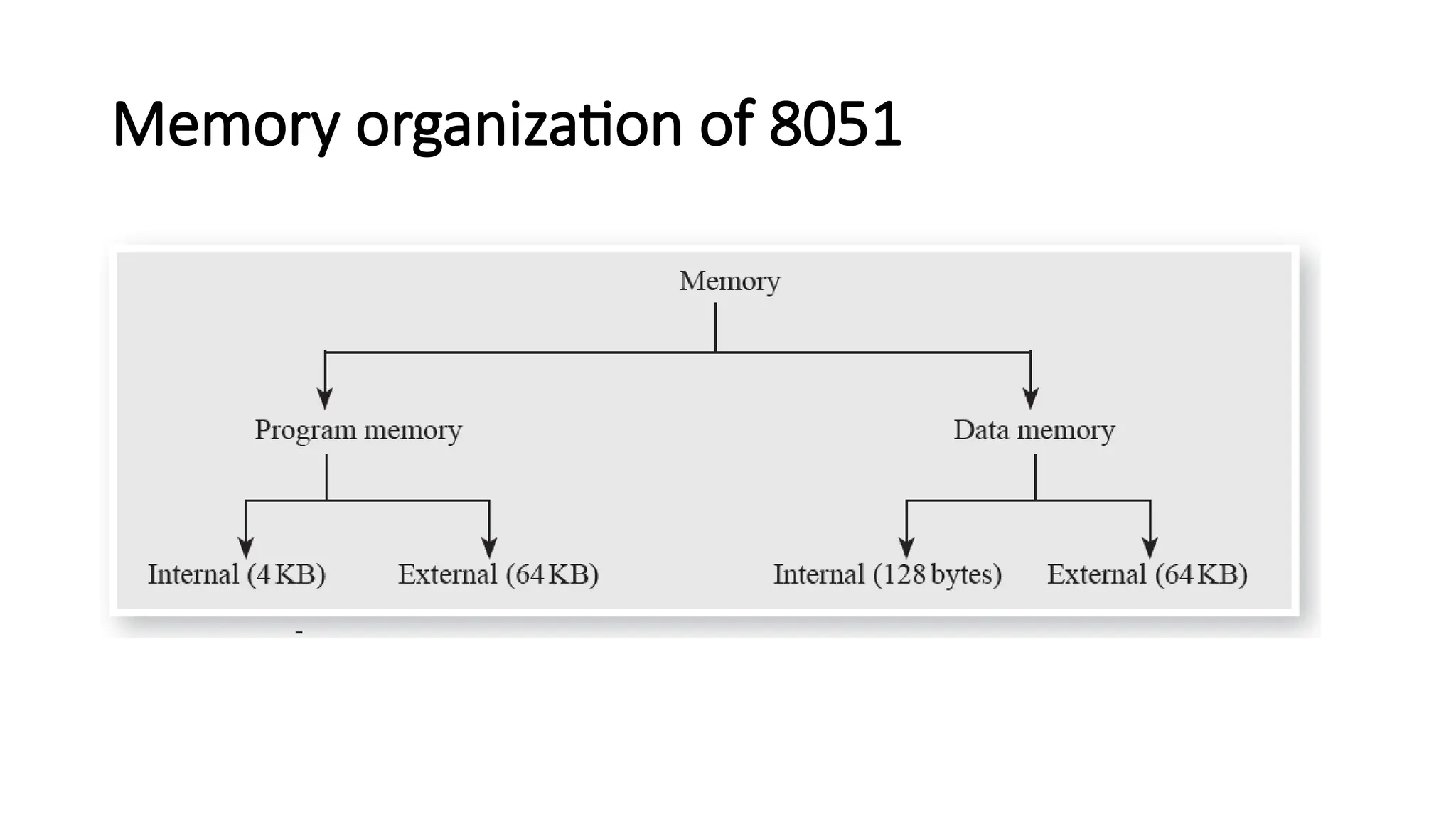
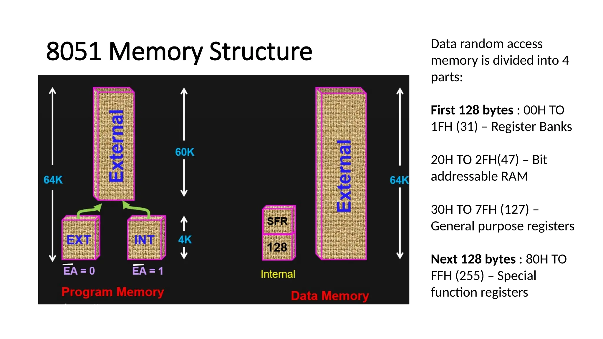
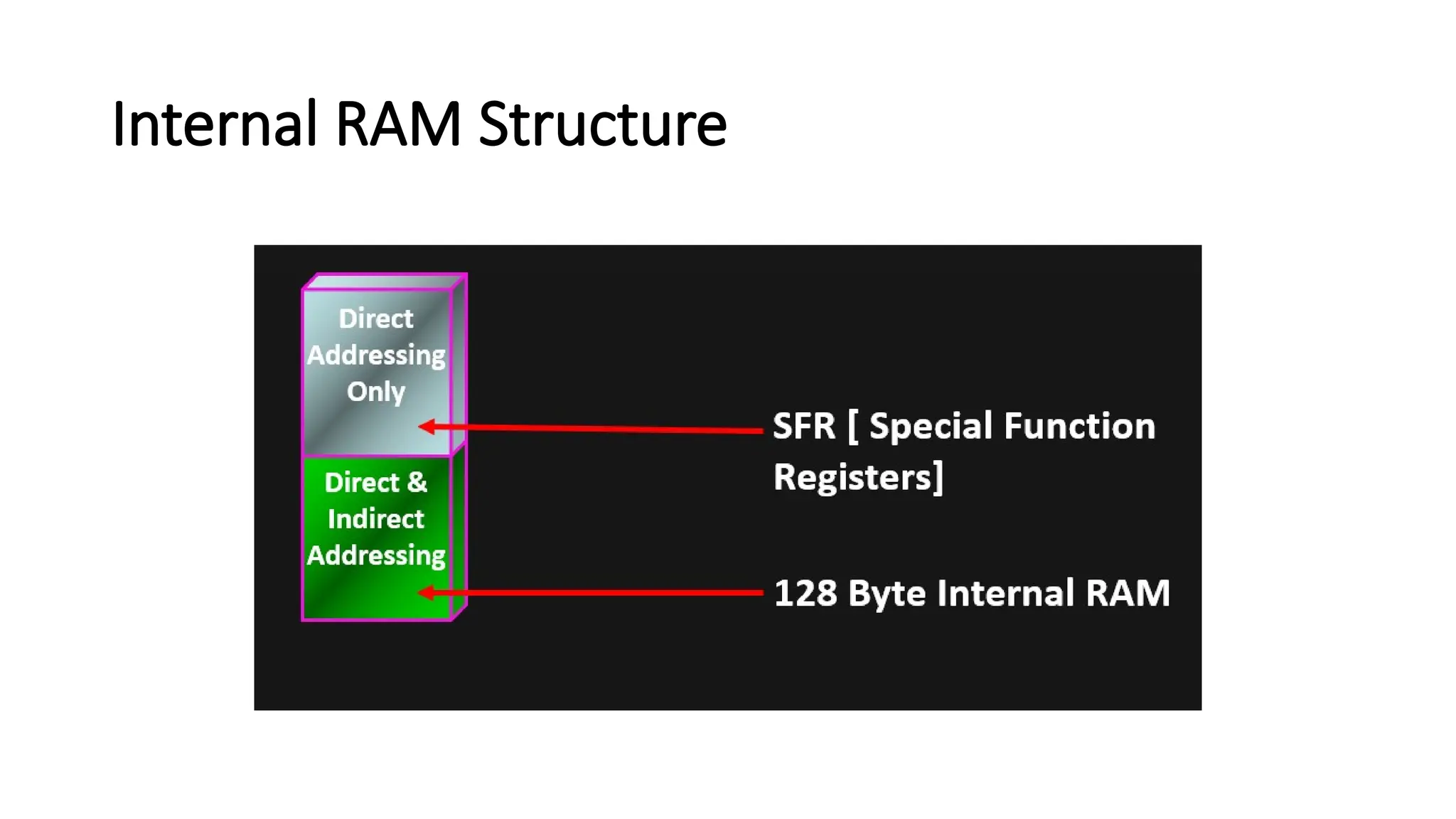
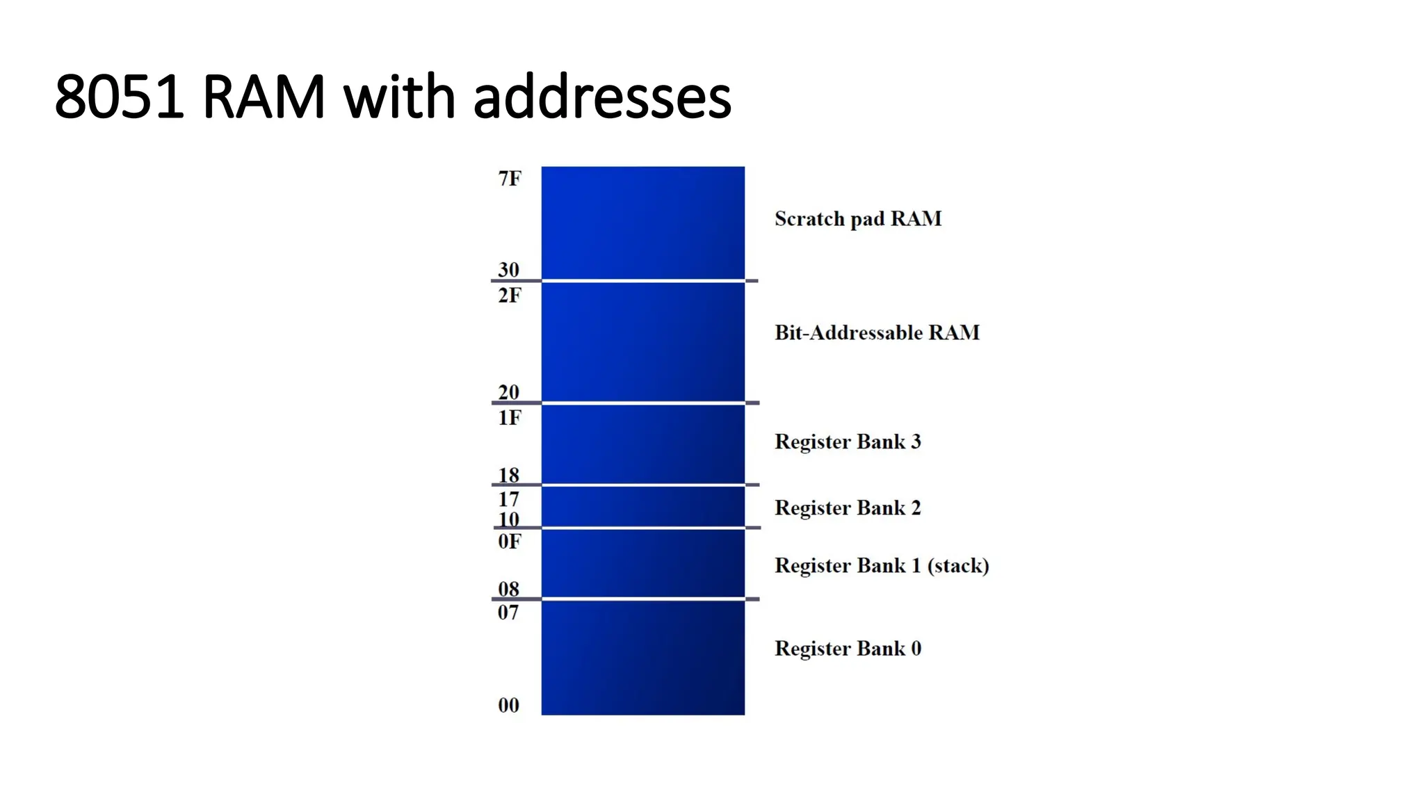
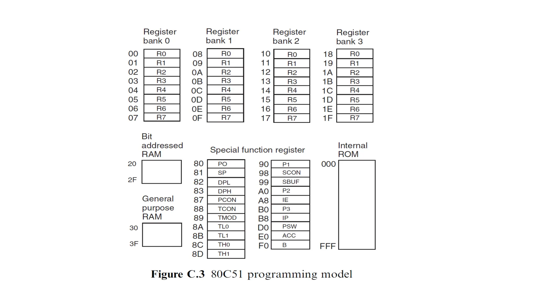
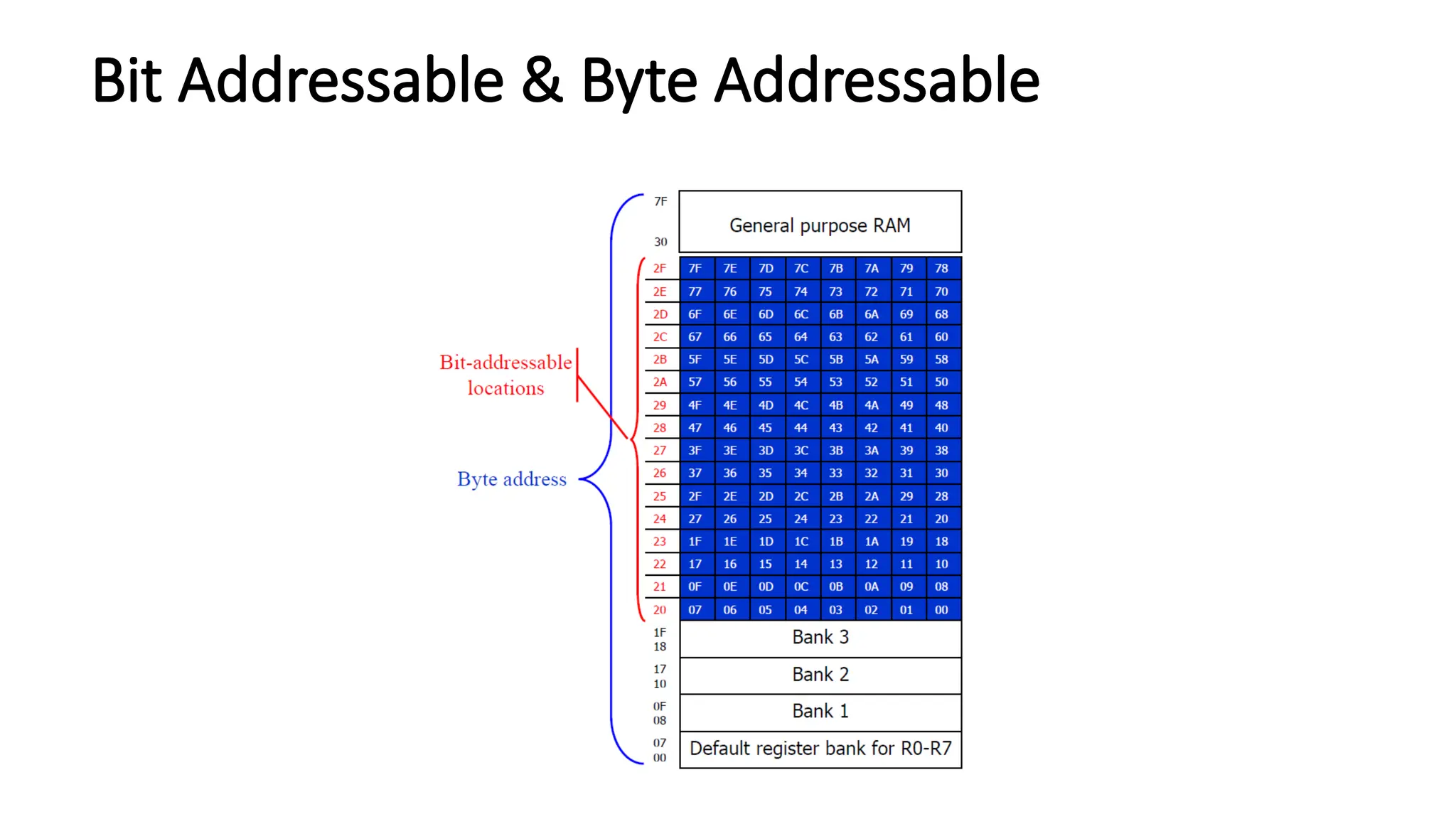
8051 Memory StructureData random access memory is divided into 4 parts: First 128 bytes : 00H TO 1FH (31) – Register Banks 20H TO 2FH(47) – Bit addressable RAM 30H TO 7FH (127) – General purpose registers Next 128 bytes : 80H TO FFH (255) – Special function registers
52.
MEMORY ORGANISATION • Inthe 8051, the memory is organized logically into program memory and data memory separately. • The program memory is read-only type; the data memory is organized as read–write memory. • Again, both program and data memories can be within the chip or outside. • The Intel 8051 has 128 bytes of RAM and 4 KB of ROM within the chip. • The address bus of the 8051 is 16 bits wide. So it can access 64 KB of memory.
53.
MEMORY ORGANISATION • Asthe memory is organized separately as program memory and data memory, the 8051 microcontroller can access 64 KB of program memory and 64 KB of data memory. • The user can configure the entire program memory outside the chip or use 4 KB inside and 60 KB outside the chip. • The internal data memory is accessed with 8-bit addresses and the external data memory with 16-bit addresses. • So the maximum data memory that can be connected to the 8051 system is 64 KB.
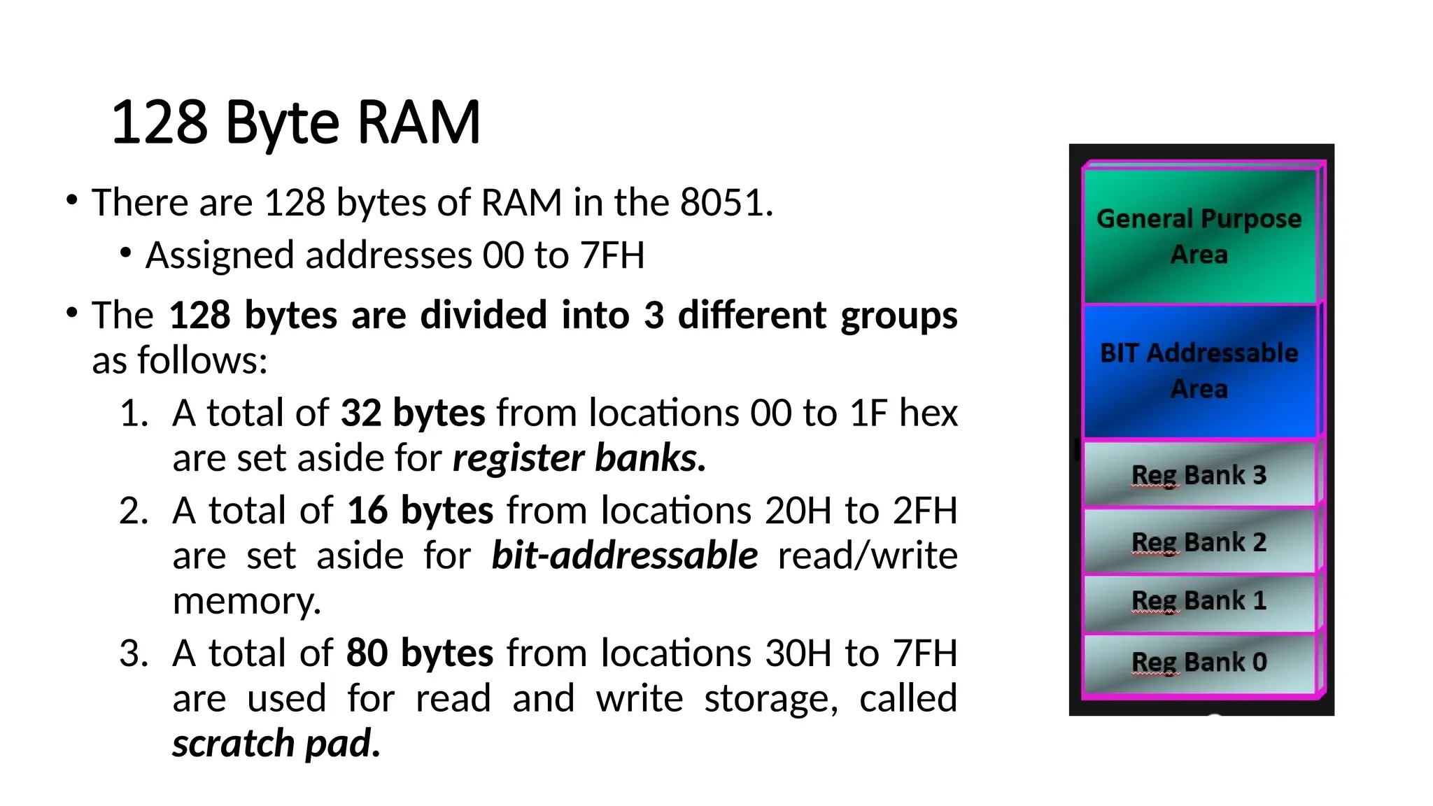
128 Byte RAM •There are 128 bytes of RAM in the 8051. • Assigned addresses 00 to 7FH • The 128 bytes are divided into 3 different groups as follows: 1. A total of 32 bytes from locations 00 to 1F hex are set aside for register banks. 2. A total of 16 bytes from locations 20H to 2FH are set aside for bit-addressable read/write memory. 3. A total of 80 bytes from locations 30H to 7FH are used for read and write storage, called scratch pad.
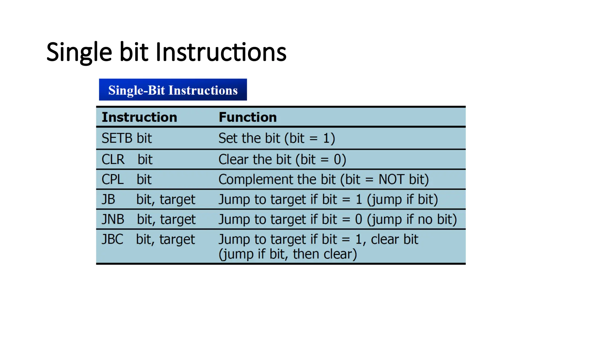
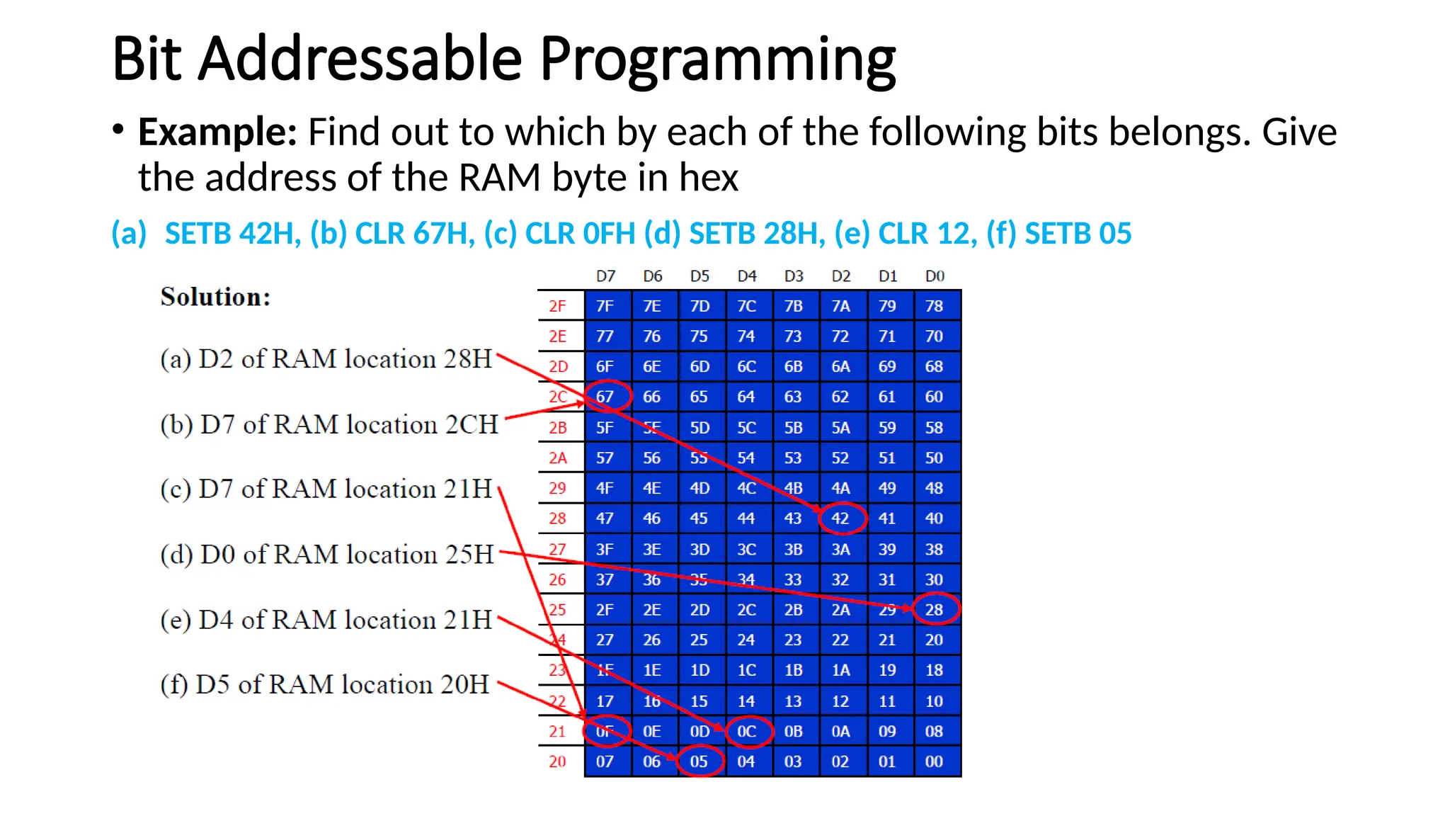
Bit Addressable Programming •Example: Find out to which by each of the following bits belongs. Give the address of the RAM byte in hex (a) SETB 42H, (b) CLR 67H, (c) CLR 0FH (d) SETB 28H, (e) CLR 12, (f) SETB 05
63.
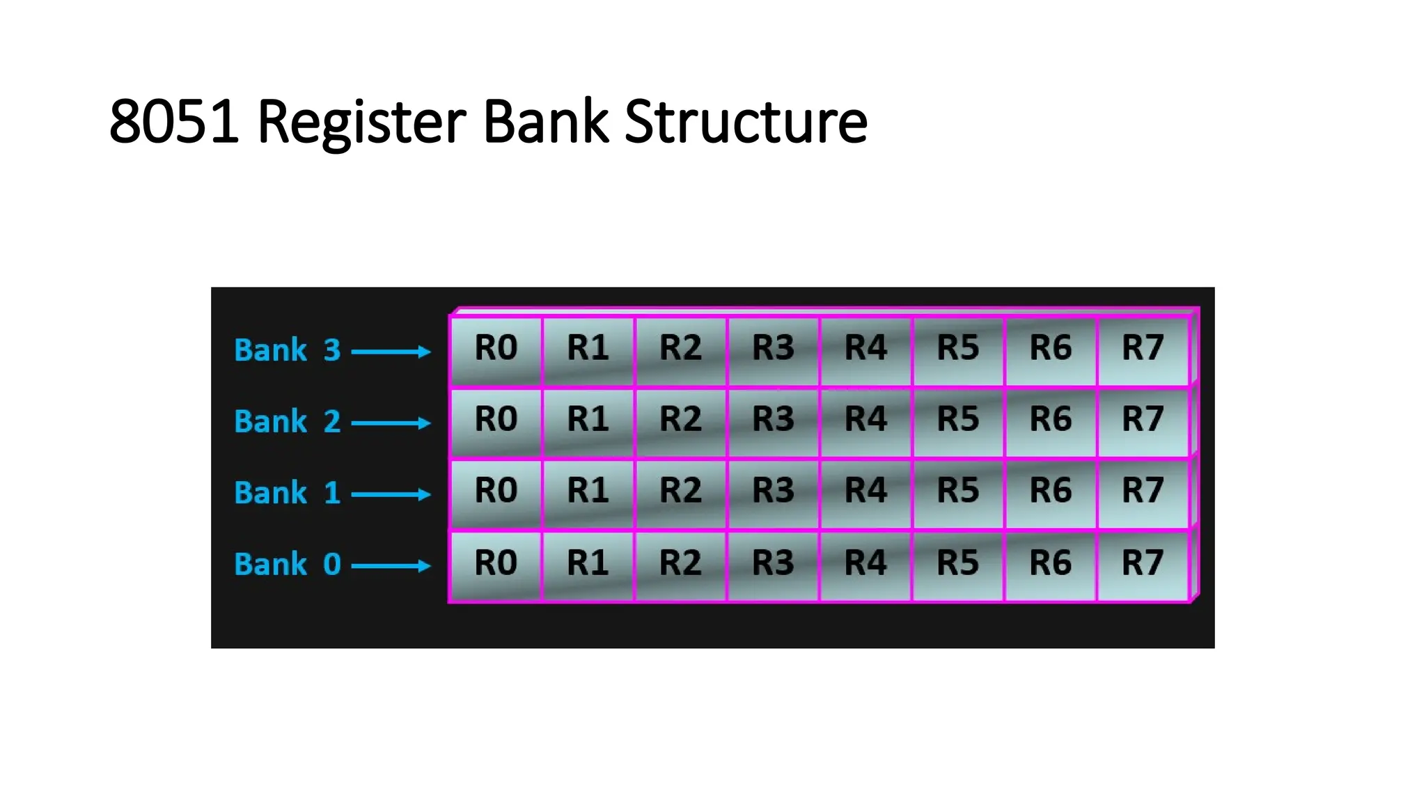
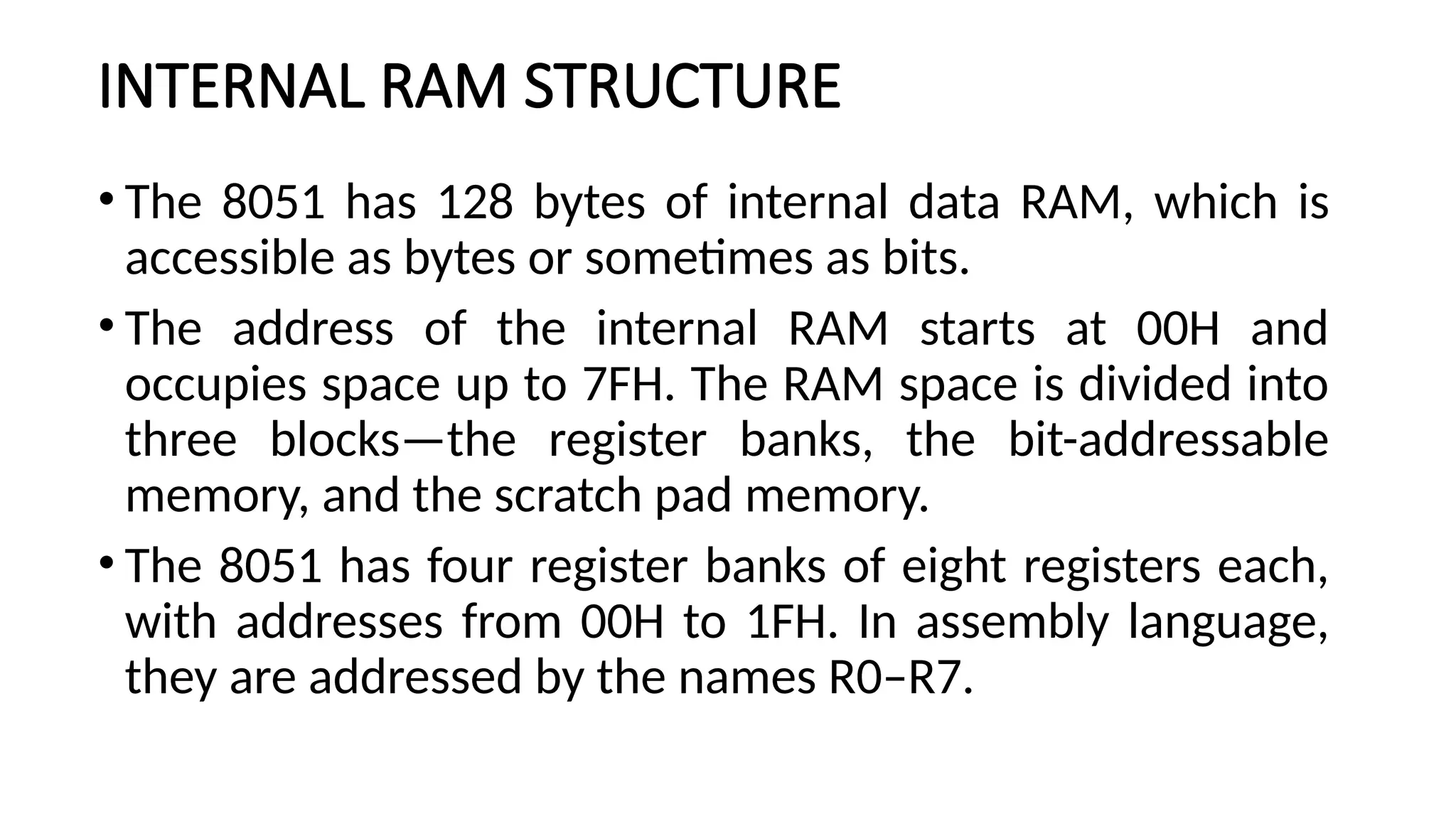
INTERNAL RAM STRUCTURE •The 8051 has 128 bytes of internal data RAM, which is accessible as bytes or sometimes as bits. • The address of the internal RAM starts at 00H and occupies space up to 7FH. The RAM space is divided into three blocks—the register banks, the bit-addressable memory, and the scratch pad memory. • The 8051 has four register banks of eight registers each, with addresses from 00H to 1FH. In assembly language, they are addressed by the names R0–R7.
64.
• The registerbanks are identified with 2 bits in the processor status word. • The PSW has two bits for identifying the register bank, i.e., 00 represents bank 0, 01 represents bank 1, 10 represents bank 2, and 11 represents bank 3. • In the 8051, bitwise operations are also possible with special instructions using the bit addresses. The bit-addressable memory is from 20H to 2FH. Bit operations are helpful in many control algorithms. • Using general-purpose scratch pad memory, programmers can read and write data at any time for any purpose. This memory ranges from the byte address 30H to the address 7FH.
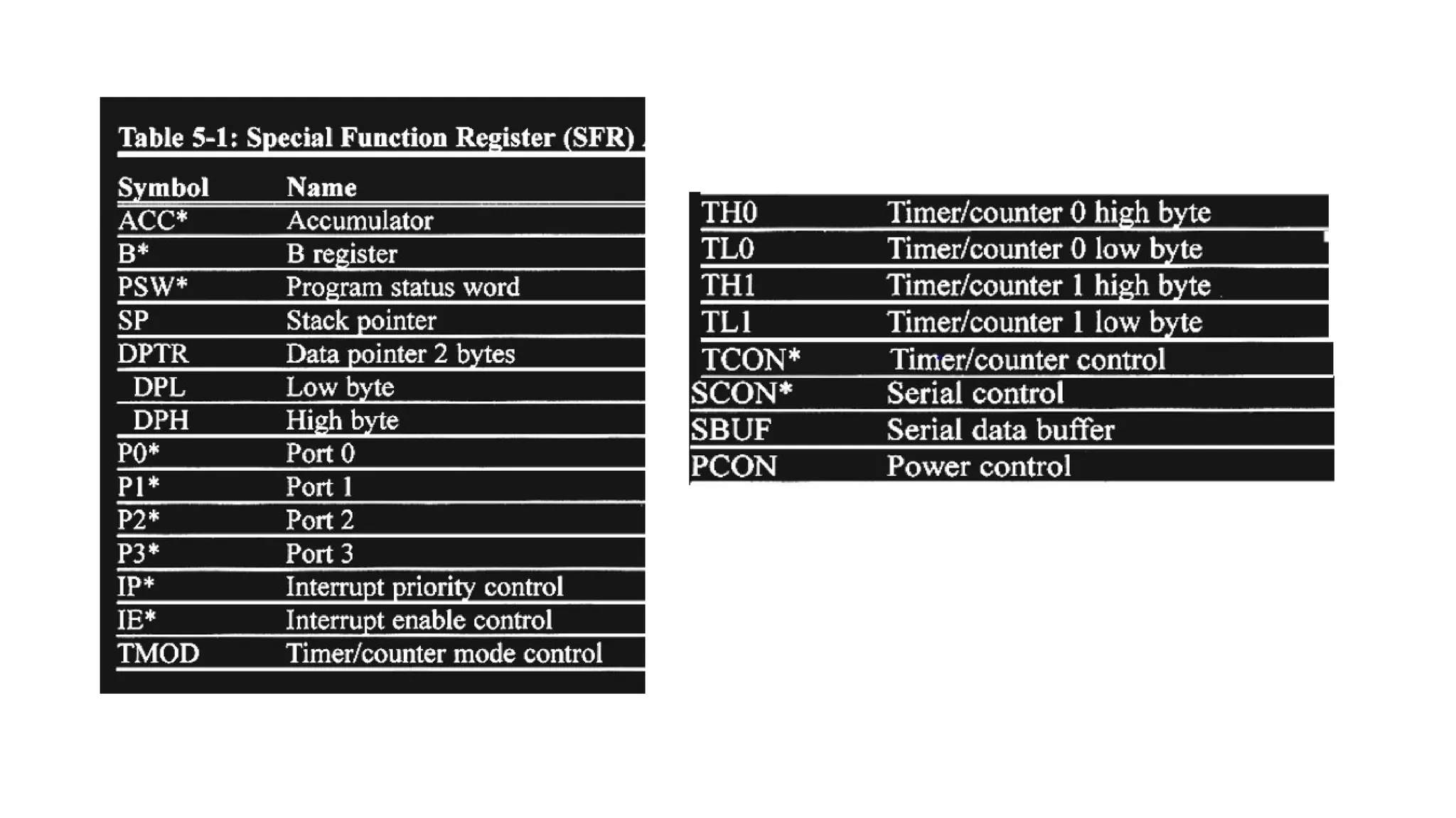
SPECIAL FUNCTION REGISTERS(SFRs) • SFR, which occupies upper 128 bytes of internal memory are the registers, that control the entire processor • They can be accessed by DIRECT addressing. • Programmers should not use the addresses in the range 80H to FFH as it is used by INTEL CORPORATION for expansion functions of 8051. • The registers available in the 8051 are as follows :
67.
LIST OF REGISTERS •Accumulators - A and B • Process Status Word - PSW • I/O port registers - P0, P1, P2, P3 • Data pointers - DPH and DPL • Serial data buffer register - SBUF • Stack pointer - SP • Timer registers - TH0, TH1 and TL0, TL1 • Timer Control Registers - TCON, TMOD • Power and Port control - PCON, SCON • Interrupt Control Registers - IP, IE.
![Program Status Word [PSW]](https://image.slidesharecdn.com/8051microcontroller-250816054347-33ebb6ff/75/8051-Microcontroller-Presentation-for-Btech-ECE-43-2048.jpg)
![Special Function Registers [SFR]](https://image.slidesharecdn.com/8051microcontroller-250816054347-33ebb6ff/75/8051-Microcontroller-Presentation-for-Btech-ECE-68-2048.jpg)