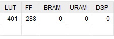
I am trying to design in VHDL a RAM model. The idea is to being able to implement the different load instructions (lb, lh and lw) present in the RISCV ISA (the overall project is to design a complete CPU).
At the end, I would like to being able to run this kind of instructions on this CPU:
uint8_t byte_var = 0x41; uint16_t halfword_var = 0xa25c; uint32_t word_var = 0x12345678; This is why I would like this RAM to provide 8-bit, 16-bit and 32-bit readings/writings.
This is purely for learning purposes and my goal is to design it from scratch (not using any already existing IP) to understand how it internally works. At end, being able to make it work in simulation is enough for me, I do not intend to implement it in a FPGA, at least for now.
I tried different designs but I don't know if there are good or bad.
First Design:
The output is a 32-bit signal. In case of a 8-bit or 16-bit writing, this signal is padded with leading 0s to get the expected 32-bit output width.
It seems to be working, however I am wondering if I am not over-complicating the RAM model. The schematic resulting from the synthesis looks quite complex to me, but I am not really familiar with usual schematics so perhaps it is actually fine.
Please find below this first design:
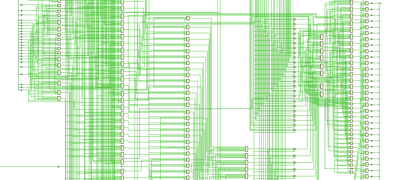
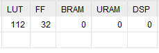
library IEEE; use IEEE.STD_LOGIC_1164.ALL; use IEEE.NUMERIC_STD.ALL; entity data_ram is port( clk : in std_logic; addr : in std_logic_vector(31 downto 0); access_width : in std_logic_vector(1 downto 0); -- "00" : illegal; "01" : 8-bit; "10" : 16-bit; "11" : 32-bit write_enable : in std_logic; data_in : in std_logic_vector(31 downto 0); data_out : out std_logic_vector(31 downto 0) ); end data_ram; architecture Behavioral of data_ram is constant RAM_SIZE_BYTES : integer := 32; type DATA_RAM_MEMORY_ARRAY_t is array (0 to RAM_SIZE_BYTES-1) of std_logic_vector(7 downto 0); signal memory : DATA_RAM_MEMORY_ARRAY_t; begin process(clk) variable index : integer; begin index := to_integer(unsigned(addr)); if rising_edge(clk) then if(index < RAM_SIZE_BYTES) then case access_width is when "00" => -- illegal value, do not write and output 0xffffffff data_out <= (others => '1'); when "01" => -- 8-bit data_out <= (31 downto 8 => '0') & memory(index); if(write_enable = '1') then memory(index) <= data_in(7 downto 0); end if; when "10" => -- 16-bit data_out <= (31 downto 16 => '0') & memory(index+1) & memory(index); if(write_enable = '1') then memory(index) <= data_in(7 downto 0); memory(index+1) <= data_in(15 downto 8); end if; when others => -- 32-bit data_out <= memory(index+3) & memory(index+2) & memory(index+1) & memory(index); if(write_enable = '1') then memory(index) <= data_in(7 downto 0); memory(index+1) <= data_in(15 downto 8); memory(index+2) <= data_in(23 downto 16); memory(index+3) <= data_in(31 downto 24); end if; end case; else data_out <= (others => '1'); end if; end if; end process; end Behavioral; This works fine it simulation, but let's see the result given by the synthesis: Here is the schematic resulting from the synthesis: 
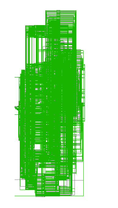
This looks too complex for only 32 bytes of storage ! This design is probably bad, although it works in the ideal case. In the real case, we would probably face some timing issues ?
Second design:
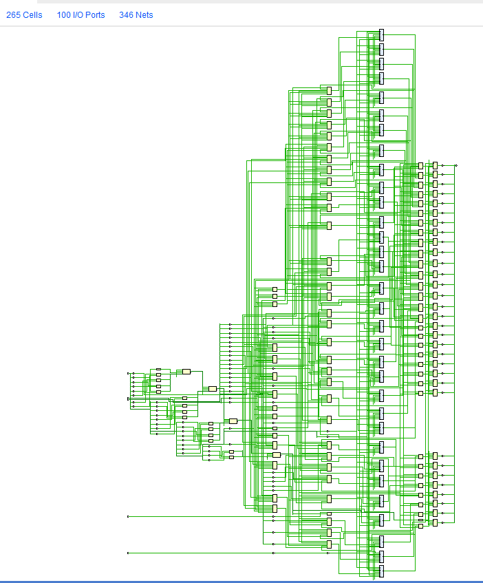
As suggested in the answers, I switched to a 32-bit wide memory instead of a 8-bit wide one.
Please find below this new design:
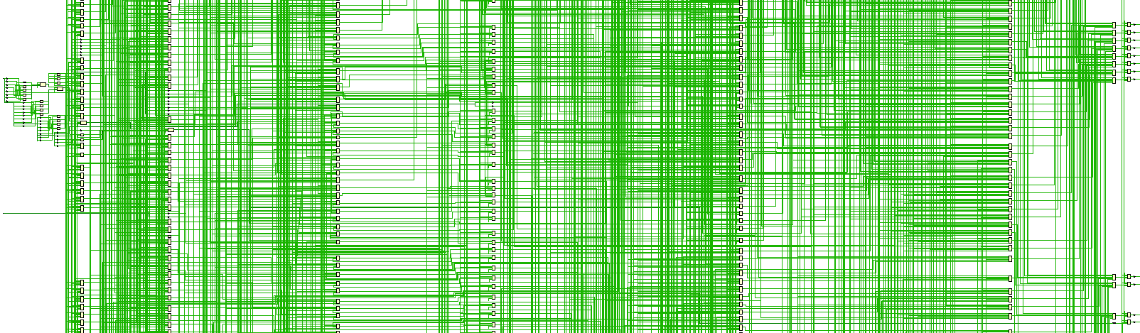
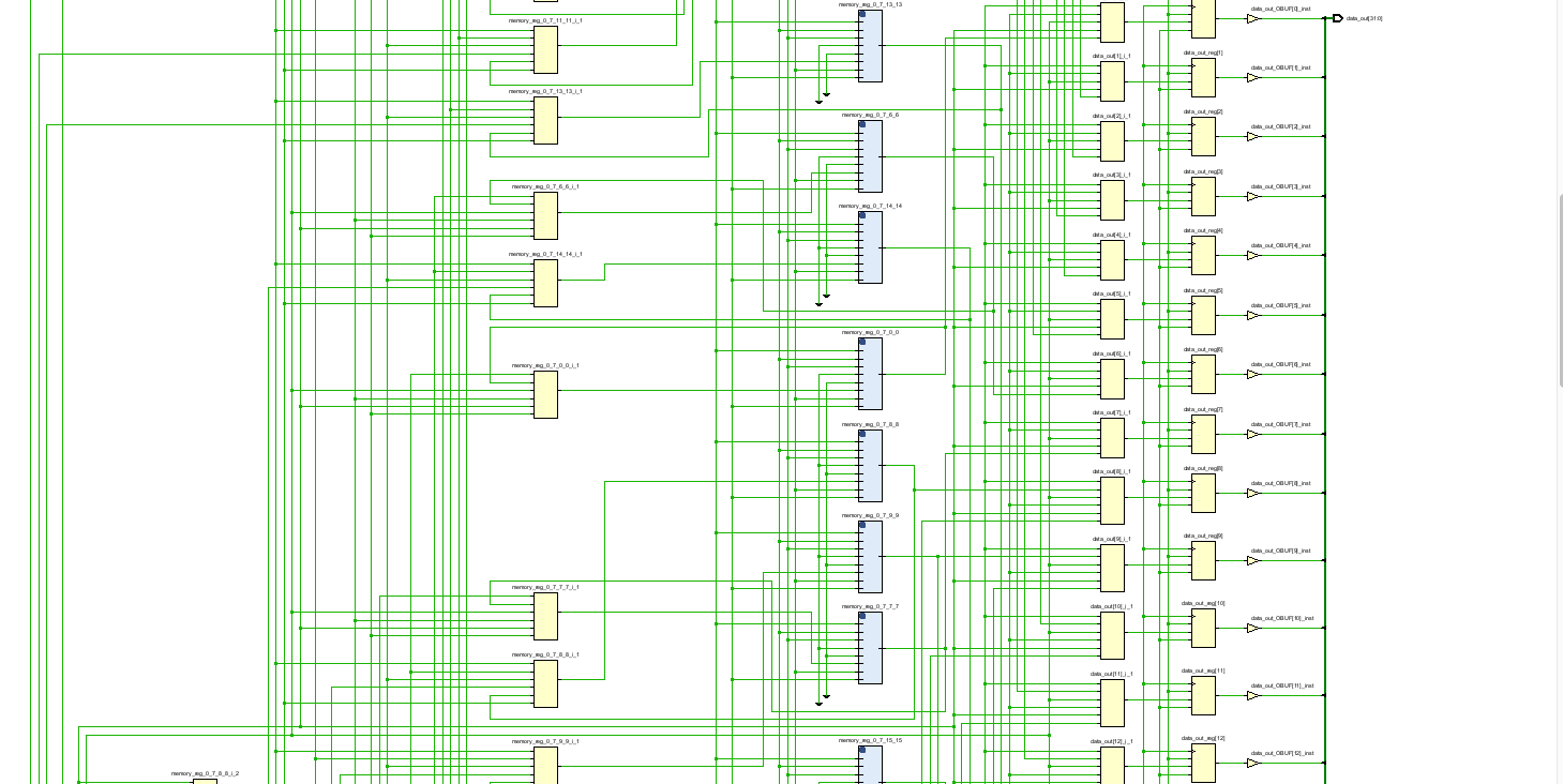
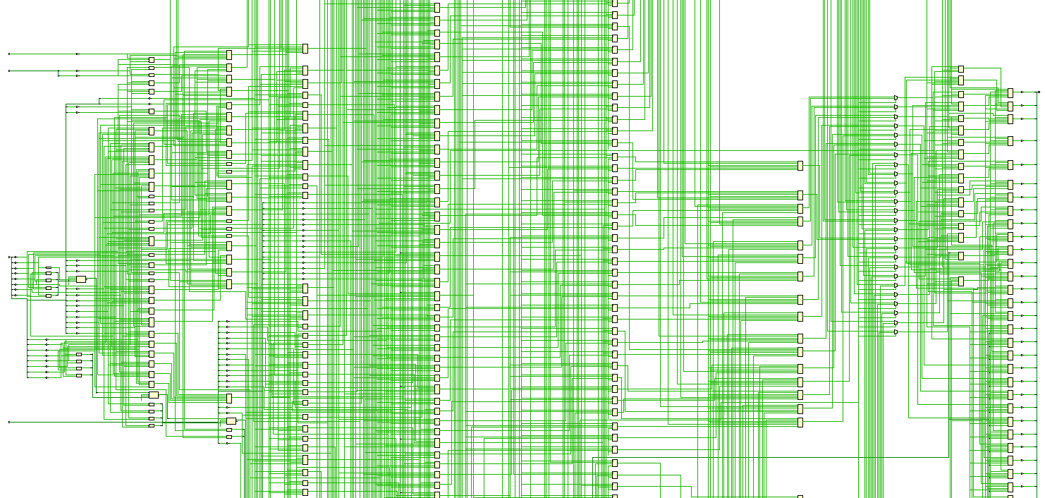
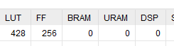
library IEEE; use IEEE.STD_LOGIC_1164.ALL; use IEEE.NUMERIC_STD.ALL; entity data_ram is port( clk : in std_logic; addr : in std_logic_vector(31 downto 0); access_width : in std_logic_vector(1 downto 0); -- "00" or "01" : 8-bit; "10" : 16-bit; "11" : 32-bit write_enable : in std_logic; data_in : in std_logic_vector(31 downto 0); data_out : out std_logic_vector(31 downto 0) ); end data_ram; architecture Behavioral of data_ram is constant RAM_SIZE_WORDS : integer := 8; type DATA_RAM_MEMORY_ARRAY_t is array (0 to RAM_SIZE_WORDS-1, 3 downto 0) of std_logic_vector(7 downto 0); signal memory : DATA_RAM_MEMORY_ARRAY_t; begin process(clk) variable word_index : integer; variable halfword_index : integer; variable byte_index : integer; begin word_index := to_integer(unsigned(addr(31 downto 2))); halfword_index := to_integer(unsigned(addr(1 downto 0) and "10")); byte_index := to_integer(unsigned(addr(1 downto 0))); if rising_edge(clk) then if(word_index < RAM_SIZE_WORDS) then case access_width is when "10" => -- 16-bit data_out <= (31 downto 16 => '0') & memory(word_index, halfword_index+1) & memory(word_index, halfword_index); if(write_enable = '1') then memory(word_index, halfword_index) <= data_in(7 downto 0); memory(word_index, halfword_index+1) <= data_in(15 downto 8); end if; when "11" => -- 32-bit data_out <= memory(word_index, 3) & memory(word_index, 2) & memory(word_index, 1) & memory(word_index, 0); if(write_enable = '1') then memory(word_index, halfword_index) <= data_in(7 downto 0); memory(word_index, halfword_index+1) <= data_in(15 downto 8); memory(word_index, halfword_index+2) <= data_in(23 downto 16); memory(word_index, halfword_index+3) <= data_in(31 downto 24); end if; when others => -- 8-bit data_out <= (31 downto 8 => '0') & memory(word_index, byte_index); if(write_enable = '1') then memory(word_index, byte_index) <= data_in(7 downto 0); end if; end case; else data_out <= (others => '1'); end if; end if; end process; end Behavioral; This design gives the same results in simulation than the previous one, but is more optimized:
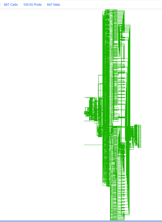
But it still looks complex, right ? 867 cells are involved for still a 8 bytes storage.
Third design:
So I tried something different. Instead of accessing the data with several indexes, I now access a full word, whatever the desired reading/writing width is, and given the desired reading/writing width, I modify this word with bit masks, and then write back this entire modified word.
library IEEE; use IEEE.STD_LOGIC_1164.ALL; use IEEE.NUMERIC_STD.ALL; entity data_ram is port( clk : in std_logic; addr : in std_logic_vector(31 downto 0); access_width : in std_logic_vector(1 downto 0); -- "00" or "01" : 8-bit; "10" : 16-bit; "11" : 32-bit write_enable : in std_logic; data_in : in std_logic_vector(31 downto 0); data_out : out std_logic_vector(31 downto 0) ); end data_ram; architecture Behavioral of data_ram is constant RAM_SIZE_WORDS : integer := 8; type DATA_RAM_MEMORY_ARRAY_t is array (0 to RAM_SIZE_WORDS-1) of std_logic_vector(31 downto 0); signal memory : DATA_RAM_MEMORY_ARRAY_t; constant byte_mask : std_logic_vector(31 downto 0) := "00000000000000000000000011111111"; constant halfword_mask : std_logic_vector(31 downto 0) := "00000000000000001111111111111111"; begin process(clk) variable word_index : integer; variable halfword_index : integer; variable byte_index : integer; variable word : std_logic_vector(31 downto 0); variable mask : std_logic_vector(31 downto 0); begin word_index := to_integer(unsigned(addr(31 downto 2))); halfword_index := to_integer(unsigned(addr(1 downto 0) and "10")); byte_index := to_integer(unsigned(addr(1 downto 0))); if rising_edge(clk) then if(word_index < RAM_SIZE_WORDS) then word := memory(word_index); case access_width is when "10" => -- 16-bit mask := std_logic_vector(shift_left(unsigned(halfword_mask), halfword_index*8)); data_out <= std_logic_vector(shift_right(unsigned(word), halfword_index*8)) and mask; if(write_enable = '1') then memory(word_index) <= (word and not mask) or (std_logic_vector(shift_left(unsigned(data_in), halfword_index*8)) and mask); end if; when "11" => -- 32-bit data_out <= word; if(write_enable = '1') then memory(word_index) <= data_in; end if; when others => -- 8-bit mask := std_logic_vector(shift_left(unsigned(byte_mask), byte_index*8)); data_out <= std_logic_vector(shift_right(unsigned(word), byte_index*8)) and mask; if(write_enable = '1') then memory(word_index) <= (word and not mask) or (std_logic_vector(shift_left(unsigned(data_in), byte_index*8)) and mask); end if; end case; else data_out <= (others => '1'); end if; end if; end process; end Behavioral; This one looks better:
As you can see, the synthezis used RAM blocks, hiding the complexity of the design inside them.
The design is probably much more efficient because it makes use of hardware features of a FPGA.
Unfortunately this is against my goal which was to understand the inner mechanism of those RAM block. So for now the best design regarding my goal is the second one, but as you have seen it is still complex and uses a lot of gates.
So I'm wondering : can we do better and improve the second design without using those RAM blocks introduced in the third design ? Or is my design ok and it is expected and usual to get such complexity in a RAM hardware ?
EDIT : as suggested in comments, FPGAs are not very well suited for implementing memory circuits, explaining the results in synthesis.
As a last edit, for info here is the most optimized design I was able to come up with, I don't think there's much optimization that can be done on this one. The main change compared to the second design above is that I put the reading outside the process and made it combinatory, and replaced variables by signals.
Fourth and last design:
library IEEE; use IEEE.STD_LOGIC_1164.ALL; use IEEE.NUMERIC_STD.ALL; use work.memory_package.all; entity data_ram is port( clk : in std_logic; addr : in std_logic_vector(31 downto 0); access_width : in MEMORY_ACCESS_WIDTH_t; write_enable : in MEMORY_ACCESS_TYPE_t; data_in : in std_logic_vector(31 downto 0); data_out : out std_logic_vector(31 downto 0) ); end data_ram; architecture Behavioral of data_ram is signal memory : DATA_RAM_MEMORY_ARRAY_t := (others => ("00000000", "00000000", "00000000", "00000000")); -- init RAM to 0 for simulation signal word_index : integer := 0; signal halfword_index : integer := 0; signal byte_index : integer := 0; begin word_index <= to_integer(unsigned(addr(31 downto 2))); halfword_index <= to_integer(unsigned(addr(1 downto 0) and "10")); byte_index <= to_integer(unsigned(addr(1 downto 0))); -- reading data_out <= -- forbidding unaligned access (others => '1') when word_index >= DATA_RAM_MEMORY_SIZE_WORDS or (access_width = MEMORY_ACCESS_WIDTH_HALFWORD and addr(0) = '1') or (access_width = MEMORY_ACCESS_WIDTH_WORD and addr(1 downto 0) /= "00") else -- 16-bit (31 downto 16 => '0') & memory(word_index, halfword_index+1) & memory(word_index, halfword_index) when access_width = MEMORY_ACCESS_WIDTH_HALFWORD else -- 32-bit memory(word_index, 3) & memory(word_index, 2) & memory(word_index, 1) & memory(word_index, 0) when access_width = MEMORY_ACCESS_WIDTH_WORD else -- 8-bit (31 downto 8 => '0') & memory(word_index, byte_index); -- writing process(clk) begin if rising_edge(clk) then if(word_index < DATA_RAM_MEMORY_SIZE_WORDS) then case access_width is when MEMORY_ACCESS_WIDTH_HALFWORD => -- 16-bit -- forbidding unaligned access if addr(0) = '0' and write_enable = MEMORY_ACCESS_TYPE_WRITE then memory(word_index, halfword_index) <= data_in(7 downto 0); memory(word_index, halfword_index+1) <= data_in(15 downto 8); end if; when MEMORY_ACCESS_WIDTH_WORD => -- 32-bit -- forbidding unaligned access if addr(1 downto 0) = "00" and write_enable = MEMORY_ACCESS_TYPE_WRITE then memory(word_index, 0) <= data_in(7 downto 0); memory(word_index, 1) <= data_in(15 downto 8); memory(word_index, 2) <= data_in(23 downto 16); memory(word_index, 3) <= data_in(31 downto 24); end if; when others => -- 8-bit if(write_enable = MEMORY_ACCESS_TYPE_WRITE) then memory(word_index, byte_index) <= data_in(7 downto 0); end if; end case; end if; end if; end process; end Behavioral; 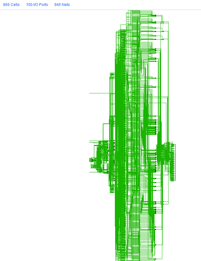
Of course for a real implementation on a FPGA, the third design is the one to use as it leverages the hardware blocks of the FPGA, resulting in a much more efficient circuit.
memoryarray has indices 0..5. Yet the read and write haveindex := to_integer(shift_left(unsigned(addr),2));. Which as far as I tell means that only indices 0 and 4 into the ``memory` array will be used. The synthesis probably recognises that, resulting in only two 32-bit memory indices being used which explains why only 64 FFs are used. Do you have a test bench to check the updated code functions as expected? \$\endgroup\$