Download to read offline

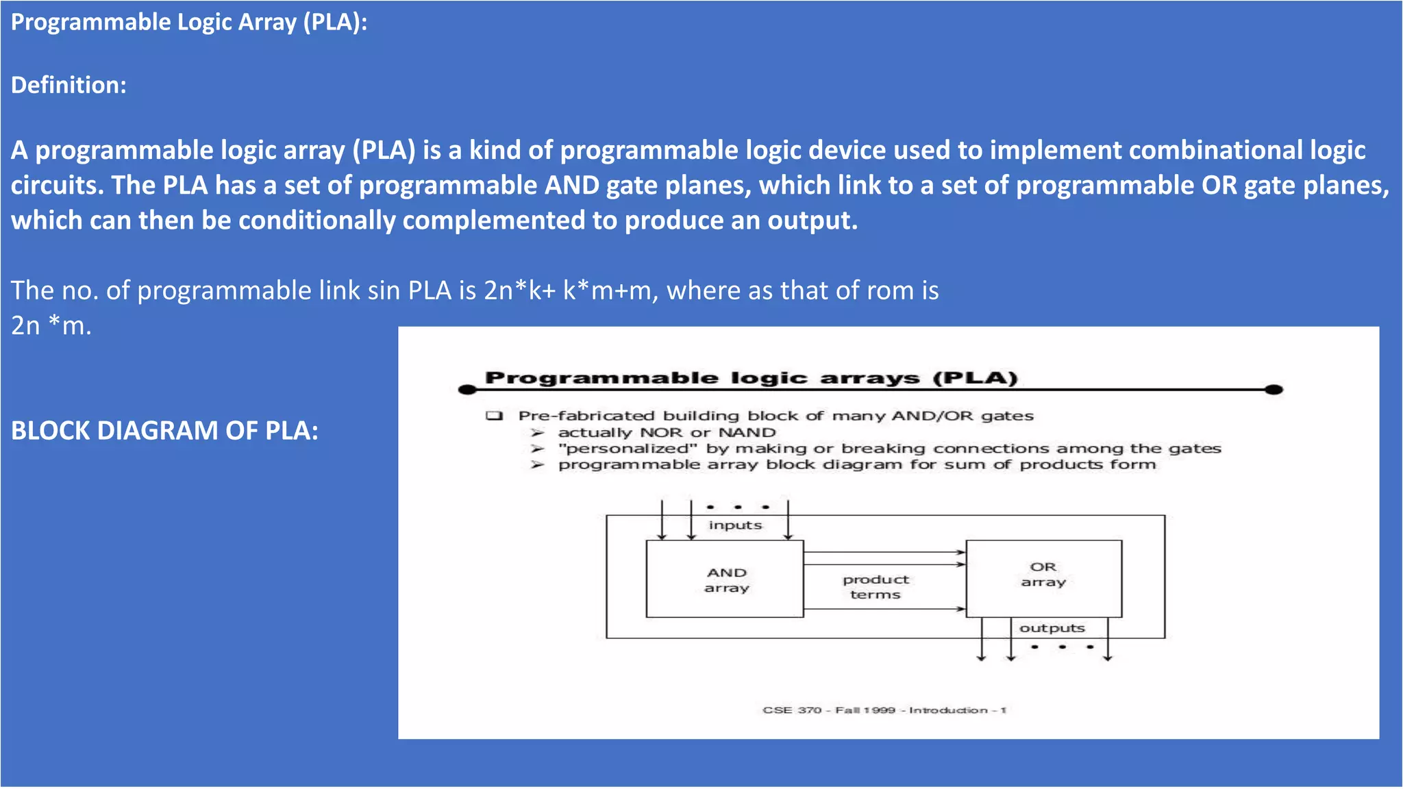
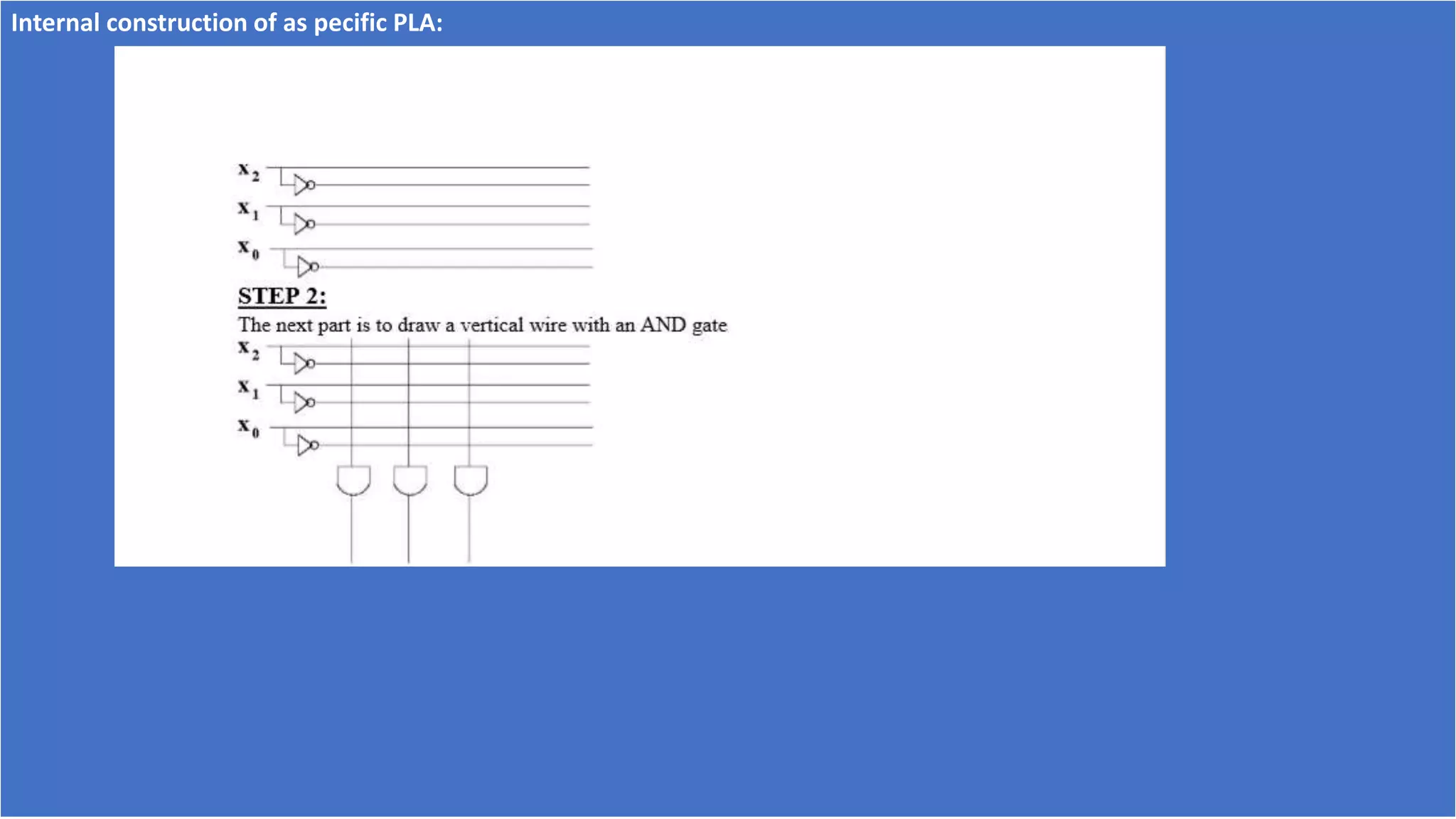
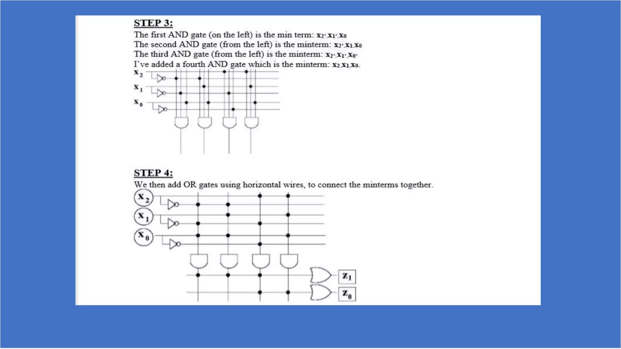
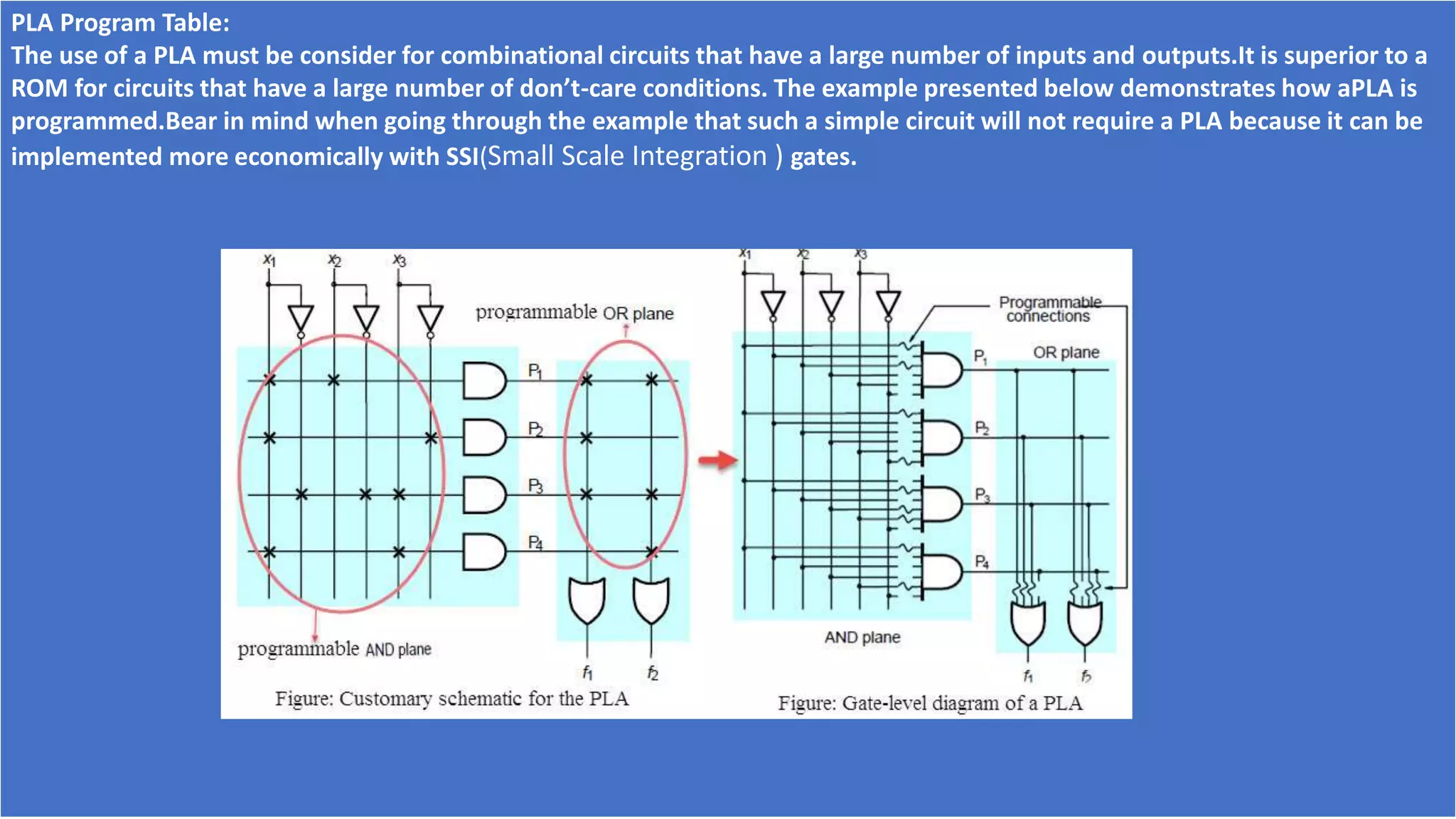
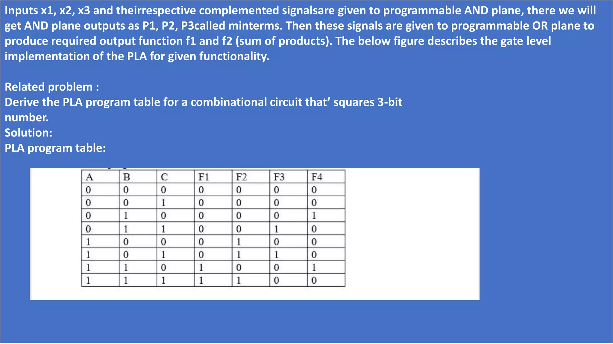
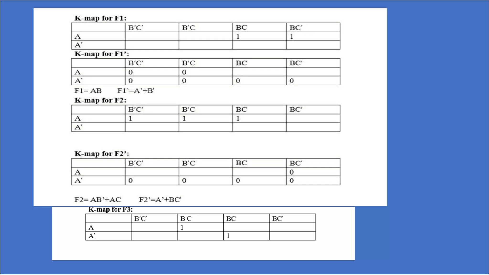
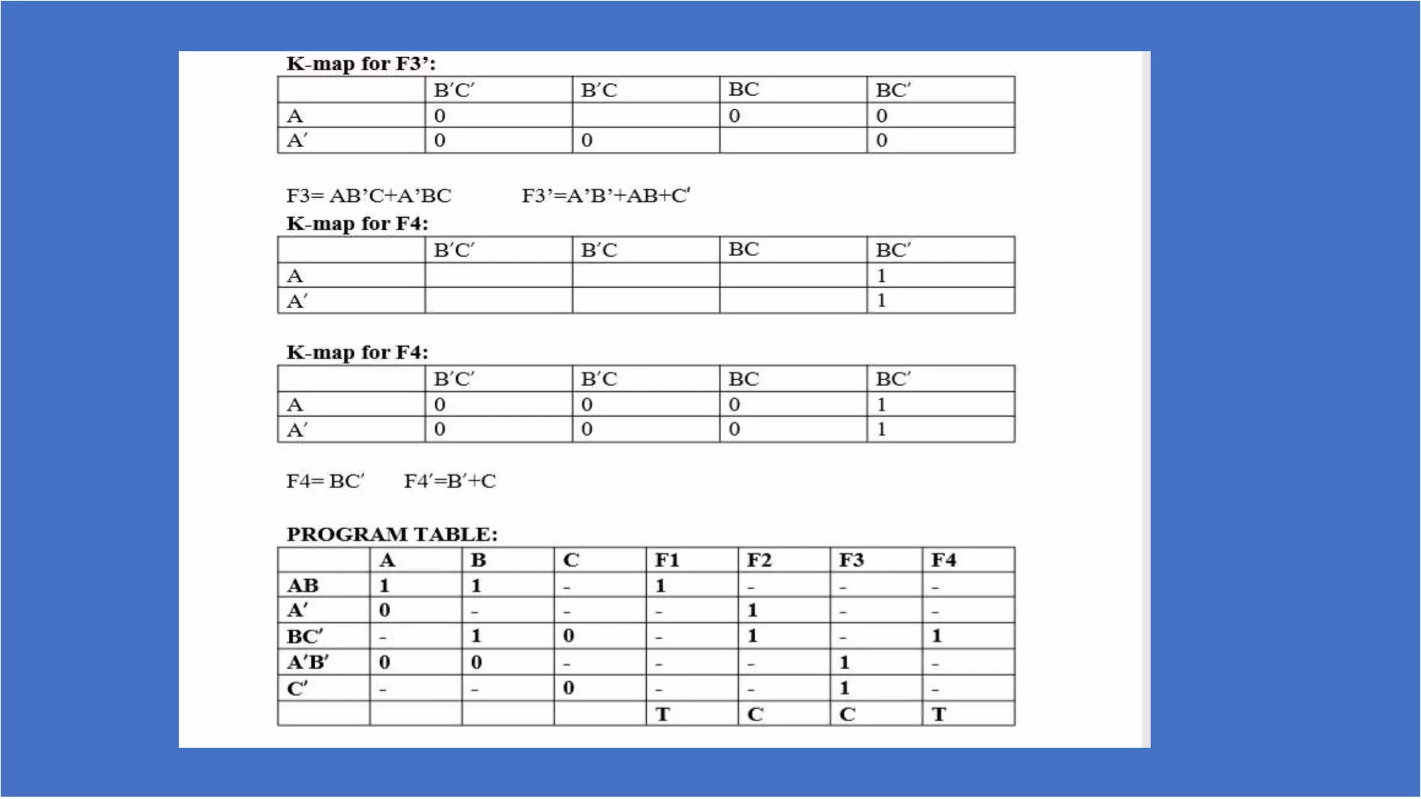

This document presents information on Programmable Logic Arrays (PLA). It defines a PLA as a type of programmable logic device used to implement combinational logic circuits. A PLA has programmable AND and OR gate planes that can be conditioned to produce outputs. The document provides the block diagram and internal construction of a PLA. It also gives examples of implementing logic functions in a PLA using a program table.