I have an slave SPI device implemented within an FPGA (Basys 3). I have had problems to route the SPI clock signal provided by a master to my slave device through one of the board PMOD pins (see this post).
What the 'application' does is: the SPI master (MCU) sends data to the slave (FPGA), and each time a byte of data is ready, the FPGA reads it and dumps the byte value to an 8 LED array. I have tried this already using routing the SPI master clock directly to the FPGA slave, and it works.
Now I want to apply the 'oversampling' technique (as explained in the post above) to avoid routing a clock signal through a PMOD pin, which is a very bad practice as far as I know. Let clk be the clock generated inside the FPGA (100 MHz), then, what I have done (which I understand is a good practice) is:
- Route the clock signal generated by the master SPI to an edge detector (within the FPGA, driven be
clk). - Drive the slave SPI with
clkas well, and check the output of the above detector in order to read/write from/in MOSI/MISO.
With the above design, the FPGA gets completely desynchronized. The value 'dumped' to the LED array makes no sense (it does work with the previous version, driving the SPI maste clock signal directly to the slave through a PMOD pin). I'm aware of the master device sends data with enough time between frames to not make the FPGA 'collapse' (I'm 100% sure about this because, as explained, the previous version I have works).
My SPI master device (which is an MCU) asserts the reset signal just after configuring the SPI master periph., so I'm sure that the problem is not that I reset the MCU and the slave is in a not valid state due to a previous SPI transaction not being completed.
I don't understand what I'm doing wrong. The code is below:
Main FPGA module
`timescale 1us/100ns // This mismatch between send and receive data size is due to the 4 dummy bits the slave // 'needs' to receive. I'm sure this works because I have tested it before trying to apply // the 'oversmaling' design. `define SEND_DATA_LENGTH 12 `define RECV_DATA_LENGTH 8 `define EN_WAIT_CYCLES_VAL 100 module spi_tb_fpga(CLK100MHZ, JA, LED); input wire CLK100MHZ; input wire [7:0] JA; output wire [15:0] LED; wire __fpga_clk; // // SPI var. decl. // wire miso, mosi, ss, sck; // SPI slave reg [`SEND_DATA_LENGTH - 1 : 0] slave_send_data = 12'hf55; wire [`RECV_DATA_LENGTH - 1 : 0] slave_recv_data; reg [`RECV_DATA_LENGTH - 1 : 0] slave_recv_buff = 0; reg [7:0] slave_read_val = 0; wire slave_recv_data_rdy; reg clk = 0; wire rst; spi_slave sl( miso, mosi, ss, sck, slave_send_data, slave_recv_data, slave_recv_data_rdy, __fpga_clk, rst ); assign __fpga_clk = CLK100MHZ; // slave_read_val is a buffer set by the SPI slave each time it finishes reading 8 + 4 bits // (the last 4 are dummy bits to provide more clock cycles, see below) assign LED[0] = slave_read_val[0]; assign LED[1] = slave_read_val[1]; assign LED[2] = slave_read_val[2]; assign LED[3] = slave_read_val[3]; assign LED[4] = slave_read_val[4]; assign LED[5] = slave_read_val[5]; assign LED[6] = slave_read_val[6]; assign LED[7] = slave_read_val[7]; // JA is the PMOD header 0 assign JA[0] = mosi; assign JA[2] = ss; assign JA[3] = sck; assign JA[4] = rst; // // Capture SPI rx buffers // always @ (posedge slave_recv_data_rdy) begin slave_read_val <= slave_recv_data[7:0]; end endmodule Edge detectors
module pos_edge_det ( input wire sig, input wire clk, output wire pe); reg sig_dly; always @ (posedge clk) begin sig_dly <= sig; end assign pe = sig & ~sig_dly; endmodule module neg_edge_det ( input wire sig, input wire clk, output wire pe); reg sig_dly; always @ (posedge clk) begin sig_dly <= sig; end assign pe = sig | ~sig_dly; endmodule SPI slave device
The SPI slave is supposed to read 8 bits + 4 dummy bits that are there just to provide the device enough clock cycles to finish all its work. I'm aware of this is no longer necessary given that it now receives the main FPGA clock, but I want to focus on the de-synchronization problem.
The SPI module (see bottom of the snippet below) instantiates both tx and rx, but tx can be ignored since I'm only testing the rx part for now.
module spi_slave #(parameter SEND_DATA_LEN = 12, parameter RECV_DATA_LEN = 8)( output wire miso, input wire mosi, input wire ss, input wire sck, input wire [SEND_DATA_LEN - 1 : 0] send_data, output wire [RECV_DATA_LEN - 1 : 0] recv_data, output wire recv_data_rdy, input wire clk, input wire rst ); wire psck; wire nsck; wire prst; pos_edge_det ped_psck(sck, clk, psck); neg_edge_det ned_psck(sck, clk, nsck); pos_edge_det ped_rst(rst, clk, prst); spi_tx #(.DATA_LENGTH(SEND_DATA_LEN)) tx(miso, ss, nsck, send_data, prst, clk); spi_rx #(.DATA_LENGTH(RECV_DATA_LEN)) rx(mosi, ss, psck, recv_data, recv_data_rdy, prst, clk); endmodule module spi_rx #(parameter DATA_LENGTH = 8)( input wire rx, input wire ss, input wire sck, output reg [DATA_LENGTH - 1 : 0] data, output reg data_rdy, input wire prst, input wire clk ); localparam IDLE = 0, RECV = 1, DUMMY_BITS = 2; reg [DATA_LENGTH - 1 : 0] buff = 0; reg [3:0] idx = 0; reg [3:0] dummy_bits_cnt = 0; reg [4:0] timer = 0; reg [1:0] cs = IDLE; initial begin data <= 0; data_rdy <= 0; end always @ (posedge clk or posedge prst) begin if (prst) begin buff <= 0; idx <= 0; dummy_bits_cnt <= 0; timer <= 0; cs <= IDLE; data <= 0; data_rdy <= 0; end else if (sck) begin case (cs) IDLE: begin if (!ss) begin cs <= RECV; data_rdy <= 0; data <= 0; buff[idx] <= rx; idx <= idx + 1; dummy_bits_cnt <= 0; end end RECV: begin idx <= idx + 1; if (idx >= DATA_LENGTH) begin data <= buff; buff <= 0; idx <= 0; cs <= DUMMY_BITS; end else begin buff[idx] <= rx; end end DUMMY_BITS: begin if (!data_rdy) data_rdy <= 1; dummy_bits_cnt <= dummy_bits_cnt + 1; if (dummy_bits_cnt == 2) begin cs <= IDLE; end end endcase end end endmodule 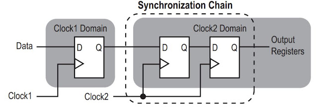
@(posedge slave_recv_data_rdy)block - usually edge sensitivity is done on a clock. You can use the clock edge, andif (slave_recv_data_rdy) begin.... \$\endgroup\$